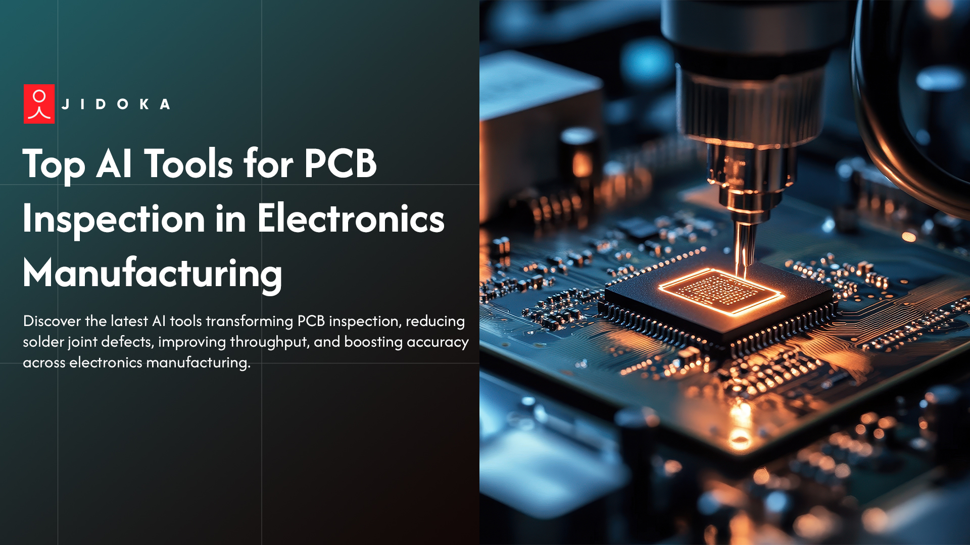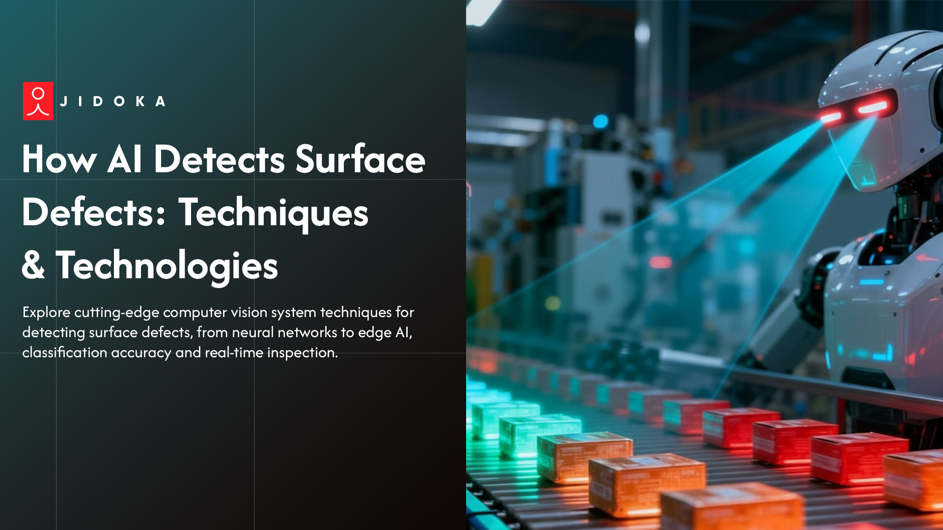
Manufacturing faces constant pressure from surface defects like scratches, cracks, stains, and inclusions that threaten product quality across automotive, electronics, steel, and FMCG sectors. A modern computer vision system powered by AI catches these flaws in real time, minimizing waste and boosting uptime.
Recent advances have revolutionized surface defect AI techniques through bio-inspired vision sensors and 3D machine vision systems. Advanced neural networks like YOLOv11 achieve 93.4% validation accuracy, while attention-guided fusion networks process multi-scale features with precision.
Modern imaging algorithms incorporate transformer models and feature fusion techniques for defect classification accuracy exceeding 99%. Anomaly detection methods use synthetic learning with minimal labeled data, while saliency detection highlights defect regions across high-speed production lines.
Technologies like Jidoka apply these advanced techniques to deliver turnkey inspection solutions with proven manufacturing results.
This exploration demonstrates how forward-thinking manufacturers can implement these technologies for defect-free production excellence.
How AI-Powered Computer Vision System Works to Detect Surface Defects
Image Acquisition & Pre-Processing
Manufacturing environments demand robust data capture systems that handle diverse lighting conditions and material variations. Current computer vision system implementations utilize:
- High-resolution cameras up to 8K resolution with consistent LED lighting arrays
- HDR imaging capabilities for extreme contrast scenarios
- Bio-inspired vision sensors capturing per-pixel brightness changes asynchronously
- 3D machine vision systems with laser triangulation and structured light projection
These event-based cameras excel at detecting weak defects through energy difference detection principles, outperforming traditional frame-based approaches. Surface defect AI techniques benefit from precise depth information for irregular surface geometries found in aerospace components and precision bearings.
Multi-spectral imaging and polarization techniques actively suppress glare interference on highly reflective surfaces. Advanced pre-processing algorithms normalize lighting variations, enhance contrast ratios, and prepare image data for neural networks analysis, ensuring consistent validation accuracy across production shifts.
Imaging Algorithms & Feature Extraction
Processing captured images requires sophisticated imaging algorithms that isolate potential defect regions while suppressing background noise. Current surface defect AI techniques employ:
- Saliency detection methods highlighting areas of interest
- Attention-guided fusion networks like JAFFNet and BEG-YOLO with CSP-GFPN architectures
- Multi-scale feature extraction using Detail-directional Fusion Modules (DDFM)
- Spatial-shifted MLP integration for long-range dependency capture
Dual-branch feature extraction architectures combine semantic understanding with structural detail processing. Cross Aggregation Nodes (CAN) ensure semantic consistency across pyramid levels while reducing information redundancy. These feature fusion approaches enable precise small defect localization even in complex textured backgrounds.
Advanced transformer models process global context information, while convolutional branches capture fine-grained local details. This foundation enables the sophisticated AI techniques that power modern defect classification systems.
AI Techniques for Accurate Surface Defect AI Techniques
Neural Network Architectures
Modern manufacturing demands neural networks that balance accuracy with processing speed. Current state-of-the-art architectures include:
- YOLOv11 variants (n, s, m, l, x) achieving 88.53-93.4% mAP@0.5 on industrial datasets
- Hybrid CNN-transformer networks like Defect Transformer and MF-YOLOv11 with Focal Modulation
- BiFPN-style architectures enabling bidirectional multilevel feature fusion
- Lightweight models (SLF-YOLO, QCF-YOLO) with 37% reduced computational complexity
These optimized computer vision system architectures maintain high validation accuracy while supporting real-time inspection requirements on resource-constrained hardware platforms across diverse manufacturing environments.
Semi-supervised & Memory-based Methods
Training surface defect AI techniques with limited labeled data requires innovative approaches:
- MemSeg architectures with memory pools for pattern recognition
- SA-GAN synthetic anomaly generation creating training examples from minimal data
- MSAC-Net achieving 95.15% mDSC through multi-scale attention mechanisms
- Confident meta-learning approaches improving few-shot defect classification
These anomaly detection methods reduce training requirements while maintaining industrial-grade accuracy standards.
Transfer Learning & Data Augmentation
Surface defect AI techniques leverage:
- Advanced augmentation through SA-GAN and neural style transfer
- Fine-tuning of YOLOv11 backbones on NEU-DET and AL10-DET datasets
- Domain adaptation for cross-material detection across steel, aluminum, and composite surfaces
These sophisticated AI architectures deliver the high-performance capabilities that enable measurable validation accuracy and speed benchmarks in production environments.
Validation Accuracy & Real-Time Performance
Current surface defect AI techniques achieve unprecedented performance levels across diverse manufacturing applications. YOLOv11-based systems consistently deliver:
- F1-scores of 93.6% and AUC values approaching 0.99 on steel datasets
- mAP@0.5 values of 87.0-98.7% across different materials and defect types
- 98.7% mAP with 150 FPS throughput on hot-pressed light guide plates
- 88.9% accuracy on FPGA platforms with energy-efficient processing
Industrial performance benchmarks demonstrate sub-150ms total latency breakdown: acquisition under 50ms, inference under 50ms, and result return under 50ms. Edge-optimized models like YOLOv11-RKNN reduce detection time from 52.1ms to 33.6ms while maintaining 99.5% accuracy.
Real-time inspection requirements include dynamic threshold adaptation, continuous learning with human-in-loop feedback, and multi-scale validation accuracy across production line speeds. Processing capabilities extend up to 700 FPS on GPU platforms, with lightweight neural networks achieving 6-7 FPS on embedded CPUs.
These performance metrics enable computer vision system deployment across high-speed manufacturing environments while maintaining the precision standards required for quality assurance and defect classification reliability.
Edge AI Processing & Deployment
Edge Computing for Inspection
Modern manufacturing requires edge AI processing capabilities that operate independently of cloud infrastructure. Current deployment solutions include:
- YOLOv11-RKNN models optimized for RK3568 devices with quantization techniques
- FPGA implementations achieving 1.39× better energy efficiency than GPU platforms
- Texas Instruments AM62A processors with integrated deep learning accelerators
- Model compression reducing size from 10MB to 4MB while maintaining accuracy
Edge platforms deliver real-time processing at 3.41 GOPS/W energy efficiency, supporting millisecond inference for critical manufacturing applications. Surface defect AI techniques benefit from local processing that eliminates network dependencies and reduces response latency.
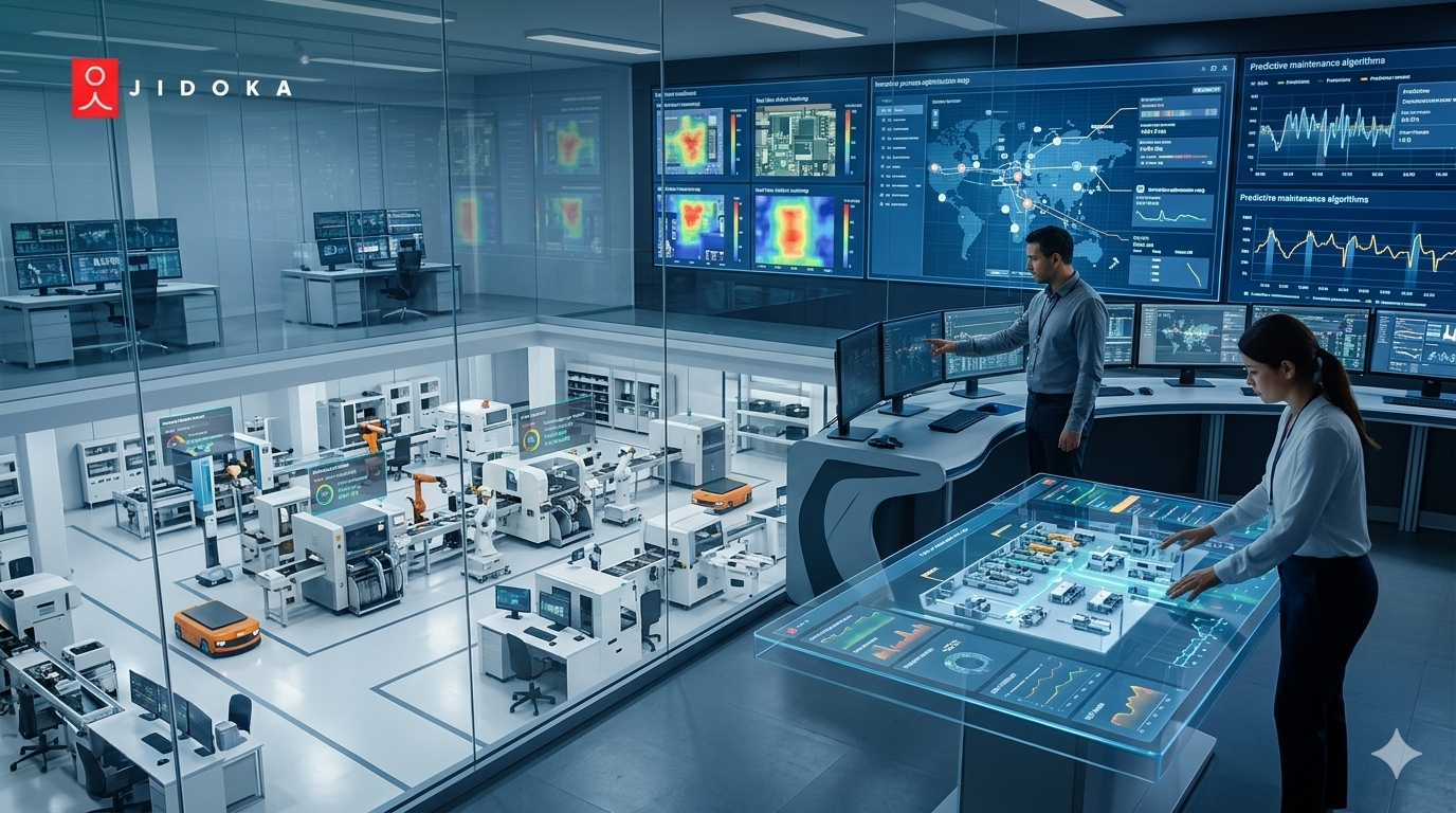
Integration & Scalability
Computer vision system deployment leverages cloud-edge-device collaborative architectures that enable:
- Seamless MES/ERP integration with existing manufacturing execution systems
- Modular hardware stacks supporting multi-line scalability across factory floors
- Wireless result transmission via ESP8266 modules for flexible installation
- Remote model updates and federated learning capabilities for continuous improvement
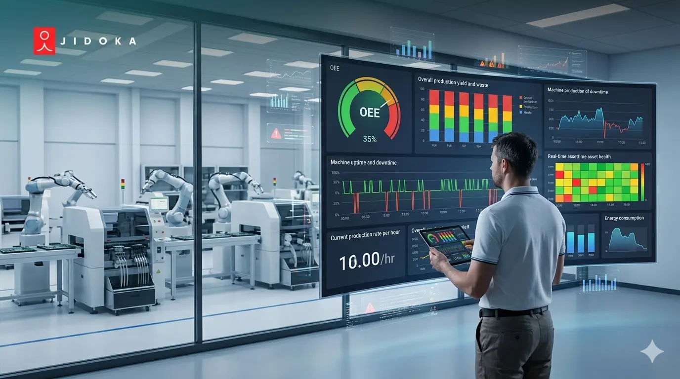
Edge AI processing supports Industry 4.0 implementations through distributed inference across factory networks. Centralized analytics dashboards provide real-time inspection monitoring with predictive maintenance scheduling, enabling manufacturers to optimize production efficiency while maintaining quality standards.
How Jidoka Can Help with Surface Defect Detection
Jidoka delivers comprehensive computer vision system solutions that combine cutting-edge hardware with proven AI methodologies. Our turnkey platforms feature:
- Modular hardware configurations supporting diverse manufacturing environments
- Pre-trained YOLOv11 models optimized for high-contrast and textured defects
- Bio-inspired sensor integration for weak defect detection capabilities
- 3D vision capabilities enabling complex surface geometry analysis
Advanced surface defect AI techniques include attention-guided fusion networks, edge deployment optimization, and multi-scale feature fusion architectures.
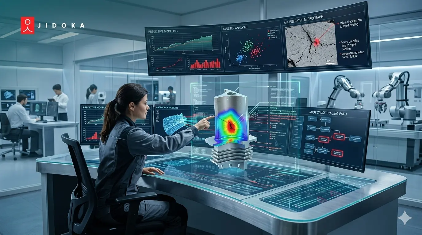
Our solutions provide defect classification dashboards with confidence scoring, validation accuracy reporting across multiple quality metrics, and human-in-loop feedback systems for continuous model improvement.
Edge-AI deployment options support FPGA and embedded processors, enabling low-latency inspection under 150ms.
Proven Track Record:
- 48+ trusted customers worldwide across global manufacturing operations
- 6 served industry verticals including automotive, FMCG, electronics, pharmaceutical, and logistics
- 100+ successful implementations with measurable quality improvements
- 300Mn+ product inspections every day demonstrating scale and reliability
Jidoka's integrated approach ensures seamless anomaly detection deployment within existing quality control workflows, delivering measurable ROI through reduced defect rates and enhanced manufacturing efficiency.
Conclusion
Manufacturing operations face mounting pressure as traditional inspection methods fail to detect microscopic surface defects across high-speed production lines. Manual quality control creates bottlenecks and human error, while existing computer vision system implementations struggle with complex textures and varying lighting conditions.
These inspection gaps trigger costly recalls, damage brand reputation, and cause production downtime. Manufacturers lose competitive advantage when defect rates exceed industry standards, making regulatory compliance increasingly difficult across global markets.
Modern surface defect AI techniques provide the solution. Bio-inspired sensors, YOLOv11 implementations, and attention-guided fusion deliver validation accuracy exceeding 99% with real-time processing. Edge-AI deployment ensures sub-millisecond response times.
Jidoka's proven anomaly detection systems eliminate these risks through advanced neural networks and transformer models. Our imaging algorithms with feature fusion support production speeds up to 700 FPS, enabling manufacturers to achieve defect-free excellence while maintaining competitive quality standards.
Contact Jidoka today to implement AI-powered surface inspection solutions that can transform your manufacturing operations.
FAQs
1. What defect types can current AI systems detect?
Modern computer vision system technologies detect scratches, cracks, stains, inclusions, misalignments, weld defects, surface oxidation, and missing components across metals, plastics, electronics, and textiles. Bio-inspired sensors and advanced neural networks capture weak contrast defects through anomaly detection methods that traditional imaging algorithms miss completely.
2. How accurate are modern detection techniques?
YOLOv11 architectures achieve 87-98.7% mAP@0.5, F1-scores of 93.6%, and AUC near 0.99 on industrial datasets. Edge-optimized models maintain 99.5% validation accuracy through attention-guided fusion, transformer models, and feature fusion techniques, ensuring reliable defect classification across diverse manufacturing environments.
3. Do systems require extensive labeled defect data?
Semi-supervised surface defect AI techniques like MemSeg and SA-GAN synthetic generation function with minimal labels via memory pooling and transfer learning. Confident meta-learning approaches reduce data requirements by 80%, enabling real-time inspection deployment without extensive neural networks training datasets or historical defect libraries.
4. Can these systems operate locally on factory floors?
Edge AI processing on FPGA platforms and RK3568 devices enables local inference with 3.41 GOPS/W efficiency and sub-150ms latency. Computer vision system deployments require no cloud dependencies, supporting real-time manufacturing through saliency detection methods while maintaining data security and eliminating network vulnerabilities.
5. What processing speeds do current systems achieve?
Lightweight networks operate at 150-700 FPS on GPU platforms, 33.6ms per image on edge devices, and 6-7 FPS on embedded CPUs. YOLOv11 variants with optimized imaging algorithms and transformer models deliver consistent validation accuracy across high-speed production lines requiring real-time inspection capabilities.
6. How do systems improve through continuous operation?
Systems support human-in-loop validation, federated learning, dynamic threshold adaptation, and continuous data feedback with remote model updates. Dashboard analytics refine validation accuracy and defect classification performance through surface defect AI techniques, anomaly detection algorithms, and feature fusion optimization based on operational manufacturing experience.