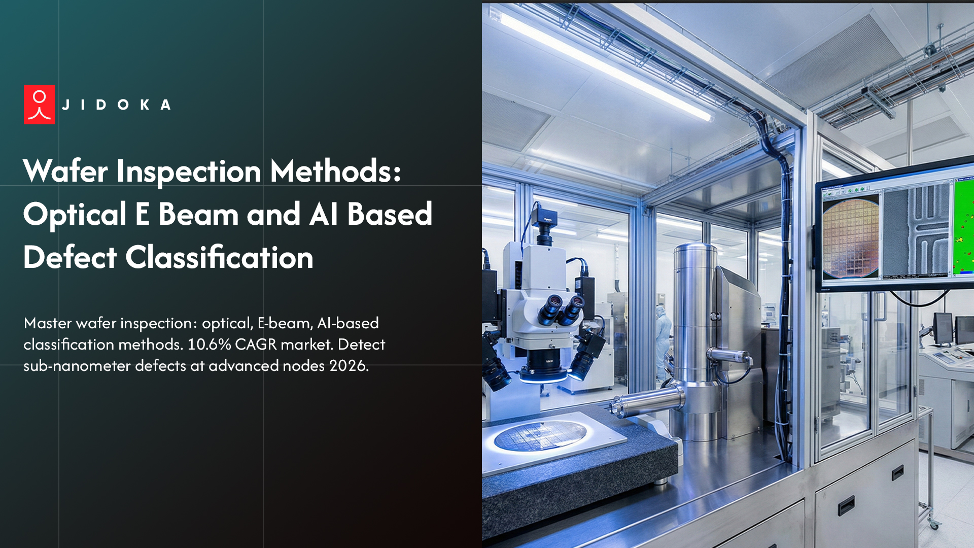
Fabricating chips at 5nm makes wafer inspection harder than ever. Defects now reach atomic scales where light fails. The market for wafer inspection grows fast.
You need tools that spot what others miss. Standard optical defect detection gives you speed. Use E-beam inspection for tiny sub-nanometer flaws. Smart fabs use AI defect classification to speed up the work.
This guide shows how semiconductor wafer inspection changes in 2026. You will learn to mix these tools for better yields and zero-defect production.
Optical Wafer Inspection: Understanding Brightfield, Darkfield, and DUV Methods
Fabs rely on light for fast wafer inspection during high-volume runs. These tools catch surface issues without touching the silicon.
1. Brightfield Inspection—The Fab Workhorse
Brightfield inspection uses 193nm light to find defects against a glowing background. It offers the best process control for surface particles and scratches. You get high throughput, but this method misses stochastic defects hidden deep in advanced nodes. It remains the standard for optical defect detection.
2. Darkfield Inspection—Enhanced Contrast for Complex Detection
Darkfield imaging hits the wafer at an angle to highlight tiny scattered light. This creates high contrast for subtle pattern errors. It is vital for semiconductor wafer inspection when you use EUV lithography. You catch more anomalies than brightfield while maintaining the speed your production line needs.
3. Deep Ultraviolet (DUV) Inspection—Advanced Node Capability
DUV tools push optical defect detection to its physical limit. These systems use short wavelengths to see features down to 65nm. While DUV helps with process control, it still cannot match electron beam technology. You use it to find bridge defects before switching to more precise methods.
Optical tools work well until defects shrink below the reach of light. To see smaller, you must switch to E-beam inspection for sub-nanometer clarity.
Electron Beam Inspection: Pushing Past Optical Limits to Sub-Nanometer Resolution
Standard optical defect detection hits a wall at the 5nm node. You need E-beam inspection to find tiny killer defects that light tools simply cannot see.
1. E-Beam Technology and Sub-Nanometer Resolution
Modern E-beam inspection hits 3nm resolution or better. This electron beam technology uses high-energy electrons to map surface and subsurface flaws. It catches tiny stochastic defects in EUV resists that cause yield loss.
- Use electron beam technology for 0.7nm detail.
- Detect electrical shorts in advanced nodes.
- Measure stochastic defects in tiny contact holes.
2. Multi-Beam E-Beam Systems—Addressing the Throughput Challenge
New multi-beam tools solve the old speed problem in wafer inspection. These systems use up to 100 columns to scan in parallel. You get a 15x speed boost for better process control during high-volume production runs.
- Scan multiple wafer areas at the same time.
- Reduce wafer inspection scan times by 90%.
- Increase total current for faster optical defect detection handoffs.
3. AI-Accelerated E-Beam: Shifting Throughput-Resolution Trade-Offs
Fabs use AI defect classification to point beams only at high-risk hotspots. This smart approach uses deep learning CNN models and chip designs to find flaws. It makes your semiconductor wafer inspection much more efficient.
- Link GDSII blueprints to E-beam inspection recipes.
- Focus on areas with high stochastic defects risk.
- Speed up automated defect classification for faster yields.
Precise hardware needs smart brains to make sense of the data. Next, you will see how AI defect classification turns these sharp images into real-time fab intelligence.
AI-Based Defect Classification: Deep Learning Transforms Inspection Intelligence
Smart software now does the heavy lifting for your fab. AI defect classification turns raw images into clear data to help you fix your wafer inspection process fast.
1. Convolutional Neural Networks for Automated Defect Recognition
deep learning CNN models recognize patterns like scratches or particles with 99% accuracy. These networks work 50x faster than humans to speed up your wafer inspection. You get consistent results across all advanced nodes without fatigue. It improves your automated defect classification significantly.
- It boosts optical defect detection accuracy.
- It identifies killer defects in milliseconds.
- It processes thousands of images per hour.
2. Automatic Defect Classification Workflow and Continuous Learning
Your automated defect classification workflow stays sharp by learning from new data. The system flags stochastic defects and updates the global library automatically. This loop improves process control over time in semiconductor wafer inspection. You can train the model with just 20 images.
- It eliminates manual data entry errors.
- It scales across multiple production lines.
- It reduces false alarms by 90%.
3. Design-Aware AI Inspection—Targeting Failure Hotspots
Design-aware AI uses chip blueprints to tell your tools exactly where to look. It links GDSII files to your wafer inspection data to find hotspots. This helps you catch stochastic defects in dense patterns. It makes your electron beam technology more efficient.
- It connects to your E-beam inspection tools.
- It targets high risk areas like dense vias.
- It shortens the time to find root causes.
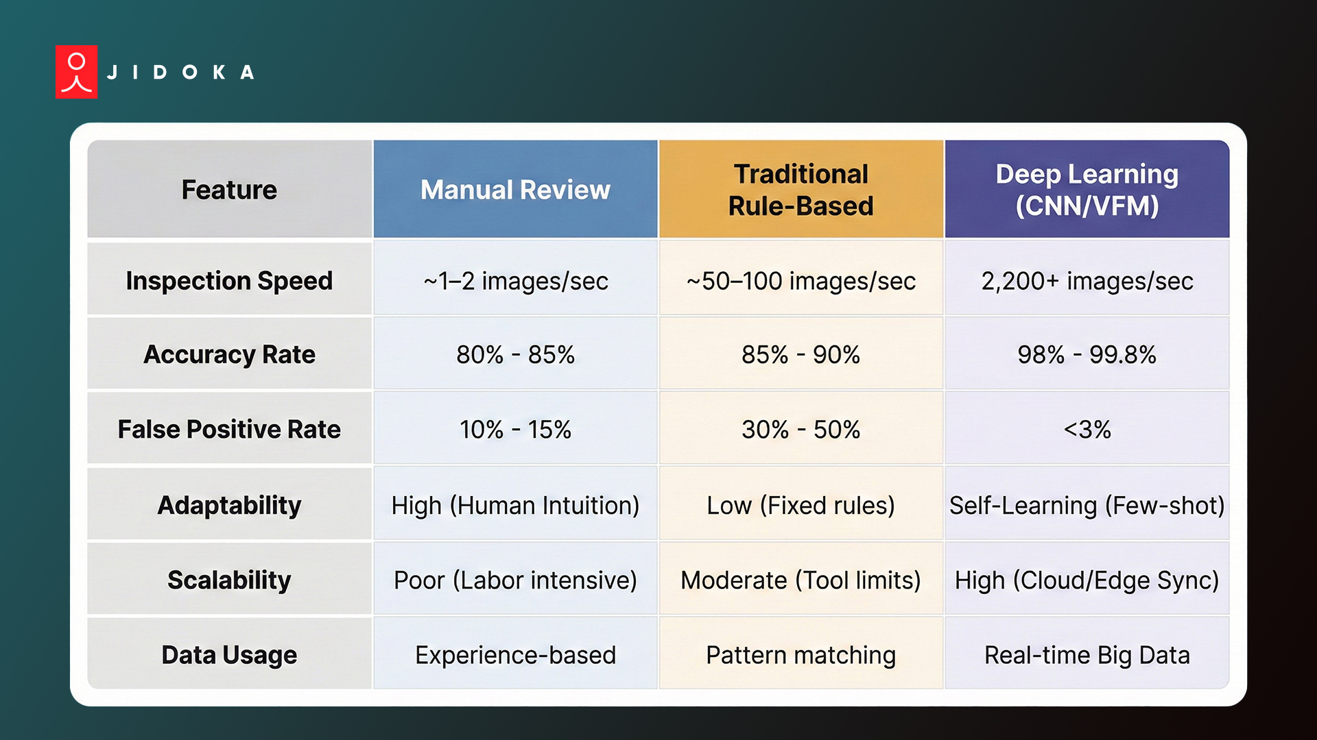
High-speed intelligence is the key to mastering 2026 manufacturing. Below is a comparison of how different AI approaches handle the pressure of semiconductor wafer inspection in 2026.
How Jidoka Tech Optimizes Wafer Inspection Workflows
Jidoka Tech provides an AI powered inspection system that thrives under production pressure. Their team aligns cameras and PLC timing so your wafer inspection stays consistent across every shift. Fabs using this setup manage 300 million inspections daily via two core tools.
- KOMPASS: This visual inspection automation tool reaches 99.8% accuracy. It reviews frames in under 10ms and learns new advanced nodes variants with 70% fewer samples.
- NAGARE: This intelligent inspection solution tracks assembly via existing cameras. It cuts rework by 35% by flagging stochastic defects or wrong sequences in real time.
Jidoka runs this automated defect detection system on local edge units to ensure your semiconductor wafer inspection remains fast and secure.
Explore Jidoka Tech to see how our AI-driven solutions can transform your factory floor.
Conclusion
Modern wafer inspection relies on mixing optical defect detection speed with E-beam inspection precision. Yet, fabs struggle with slow electron beam technology and stochastic defects that hide in advanced nodes. Missing one tiny flaw during wafer inspection leads to catastrophic yield loss and multi-billion dollar recalls.
These defects destroy your reputation and tank profits. Jidoka Tech ends this nightmare with the KOMPASS platform. By using a deep learning CNN, Jidoka automates semiconductor wafer inspection to catch every killer defect in real time.
Connect to Jidoka Tech today to bridge the gap between inspection hardware and intelligent yield optimization.
FAQs
1. Why is E-beam inspection slower than optical tools?
Electrons scan the surface pixel-by-pixel, making it much slower than light. While electron beam technology finds the smallest stochastic defects, its low throughput limits its use. Use it for critical advanced nodes where wafer inspection requires sub-nanometer precision for better yield.
2. How does AI defect classification lower production costs?
Manual review wastes time and causes errors. A deep learning CNN automates this by processing thousands of images in seconds. This automated defect classification lowers labor costs and improves process control. It ensures your semiconductor wafer inspection stays accurate without constant human intervention.
3. Do mature nodes still need E-beam inspection?
No. Most mature nodes use optical defect detection because it is faster and cheaper. You only need electron beam technology when shrinking to advanced nodes below 7nm. For larger features, high-speed wafer inspection tools provide enough process control for your manufacturing line.
4. How do stochastic defects impact semiconductor wafer inspection?
These random errors appear in EUV lithography as feature sizes shrink. Traditional optical defect detection cannot see these tiny breaks or bridges. You need E-beam inspection to find them. Identifying these stochastic defects early ensures your wafer inspection remains profitable and reliable.
5. Can AI defect classification solve "overkill" problems?
Yes. Standard machine vision inspection systems often flag harmless surface noise as errors. An intelligent inspection solution uses deep learning CNN models to filter these out. This reduces "overkill" and ensures your wafer inspection only stops for real, yield-killing flaws.