La fabricación de productos electrónicos modernos avanza rápidamente. Necesitas una calidad de impresión con estarcido perfecta para sobrevivir. Los datos muestran 60% de los problemas de SMT comienzan aquí. Encontrar un error durante la inspección de la pasta de soldadura le permite ahorrar mucho dinero. Esto evita tener que volver a trabajar más adelante.
Esta guía muestra cómo Detección de defectos SPI le ayuda a detectar pequeños errores a tiempo. Verá por qué la medición de la pasta de soldadura en 3D es imprescindible para el ensamblaje de SMT.
Hoy en día, la inspección de la pasta de soldadura mantiene alta la calidad del ensamblaje de su PCB. Utilice inspección óptica automatizada y detección de defectos en tiempo real para comprobar la medición de la altura de la pasta y detener las fallas.
Identificación de los 8 defectos críticos de la pasta de soldadura
Para mantener su línea en funcionamiento, debe saber exactamente lo que está midiendo. Los sistemas de inspección de pasta de soldadura hacen más que comprobar si hay pasta. Utilizan la medición 3D de la pasta de soldadura para trazar un mapa de cada depósito.
Esto mejora la calidad de impresión de la plantilla al detectar los errores de forma temprana. Estos son los ocho problemas principales que encuentra la detección de defectos de SPI:
Defecto de pasta de soldadura #1. Pasta insuficiente: Esto ocurre cuando la medición de la altura de la pasta cae por debajo del umbral requerido. Sin suficiente material, la junta carece de la resistencia necesaria para sobrevivir a la tensión térmica. A menudo conduce a circuitos «abiertos» en los que no existe ninguna conexión eléctrica.
Defecto de pasta de soldadura #2. Pasta excesiva: Demasiado material es tan malo como muy poco. Conduce a puente de pasta de soldadura y crea «bolas de soldadura» desordenadas que pueden rodar por la pizarra y provocar cortocircuitos aleatorios más adelante. La inspección de la pasta de soldadura mantiene el volumen entre 100 y 150 micras.
Defecto de pasta de soldadura #3. Puentes de soldadura: Esto sucede cuando la pasta conecta dos almohadillas que deben permanecer separadas. Crea un cortocircuito eléctrico inmediato. La detección de defectos mediante SPI detecta estos puentes antes de colocar los componentes, lo que evita que se produzca un fallo permanente.
Defecto de pasta de soldadura #4. Impresión offset: Si la plantilla se mueve aunque sea un poquito, la pasta no alcanza la almohadilla. Esto arruina la calidad del ensamblaje de la PCB porque el componente no queda plano. La inspección de la pasta de soldadura detecta esta desalineación antes de que la placa pase a la siguiente etapa.
Defecto de pasta de soldadura #5. Deformaciones de forma (picos): También conocidas como «orejas de perro», son puntas afiladas en la parte superior de la pasta. Ocurren cuando la espátula tira la pasta hacia arriba. Esto afecta al ensamblaje del SMT porque es posible que el componente no presione hacia abajo de manera uniforme.
Defecto de pasta de soldadura #6. Hemorragia: Cuando la pasta se extiende fuera del área de la almohadilla, se denomina sangrado. Ocurre cuando falla el sellado entre la plantilla y la pizarra. La inspección de la pasta de soldadura señala que esto representa un riesgo importante de cortocircuitos en el futuro.
Defecto de pasta de soldadura #7. Desplomándose: Esto es cuando la altura de la pasta se derrumba y el depósito se extiende después de la impresión. Suele ocurrir debido a la alta humedad o a la pasta vieja. La inspección del volumen de la pasta detecta este efecto de «fusión» antes de que se convierta en un puente.
Defecto de pasta de soldadura #8. Aberturas obstruidas: Los puntos de pegado que faltan muestran que necesitas verificar la apertura de la plantilla. Si los pequeños orificios de la plantilla se obstruyen, se producen errores de «omitir» o «no pegar». La inspección de la pasta de soldadura detecta inmediatamente estos depósitos faltantes.
La reparación de estos ocho defectos garantiza que Montaje SMT se mantiene fiable. Ahora, veamos la tecnología que hace que la inspección de la pasta de soldadura funcione tan bien.
Cómo funciona la tecnología de inspección de pasta de soldadura 3D
La inspección moderna de la pasta de soldadura hace más que simplemente tomar una foto. Crea un mapa digital de su placa. Los mejores sistemas utilizados en 2026 Perfilometría de medición de fase (PMP) para obtener resultados exactos.
Esta tecnología utiliza la luz para ver lo que pasa por alto una cámara plana. Garantiza que la calidad de impresión de su plantilla se mantenga perfecta incluso con componentes pequeños.
- Proyección de luz estructurada: La máquina proyecta patrones de luz sobre la PCB. Esto se denomina medición de pasta de soldadura 3D. Estos patrones se doblan cuando chocan con la pasta.
- Reconstrucción 3D: Las cámaras de alta velocidad observan cómo se dobla la luz. A continuación, el sistema calcula la altura, el área y el volumen total de la pasta. Esto crea un modelo 3D con una precisión submicrométrica.
- Clasificación de la IA: Los sistemas actuales utilizan Redes neuronales convolucionales (CNN) para la detección de defectos de SPI. Esta IA aprende a distinguir un defecto real de una sombra. Reduce las falsas alarmas y mantiene la línea en movimiento.
- Retroalimentación de circuito cerrado: Esta es la parte más inteligente. Si el sistema detecta que la pasta de soldadura se está uniendo o que el volumen es bajo, responde a la impresora. Puede indicarle a la impresora que ajuste la espátula o limpie la plantilla automáticamente.
Esta tecnología mantiene su ensamblaje SMT rápido y preciso. Le brinda una detección de defectos en tiempo real que los humanos simplemente no pueden igualar. A continuación, comparemos la inspección de la pasta de soldadura con la inspección óptica automatizada para ver cómo funcionan en conjunto.
SPI frente a AOI: una sinergia estratégica de calidad
Mucha gente piensa inspección óptica automatizada (AOI) puede reemplazar la inspección de la pasta de soldadura. No es así como funciona en la vida real. Estos dos sistemas son socios.
Trabajan juntos para mantener alta la calidad del ensamblaje de su PCB. Mientras SPI detecta los problemas al principio, AOI comprueba el resultado final. El uso de ambos le brinda los mejores resultados de ensamblaje de SMT.
Comparación de SPI y AOI en la línea SMT:
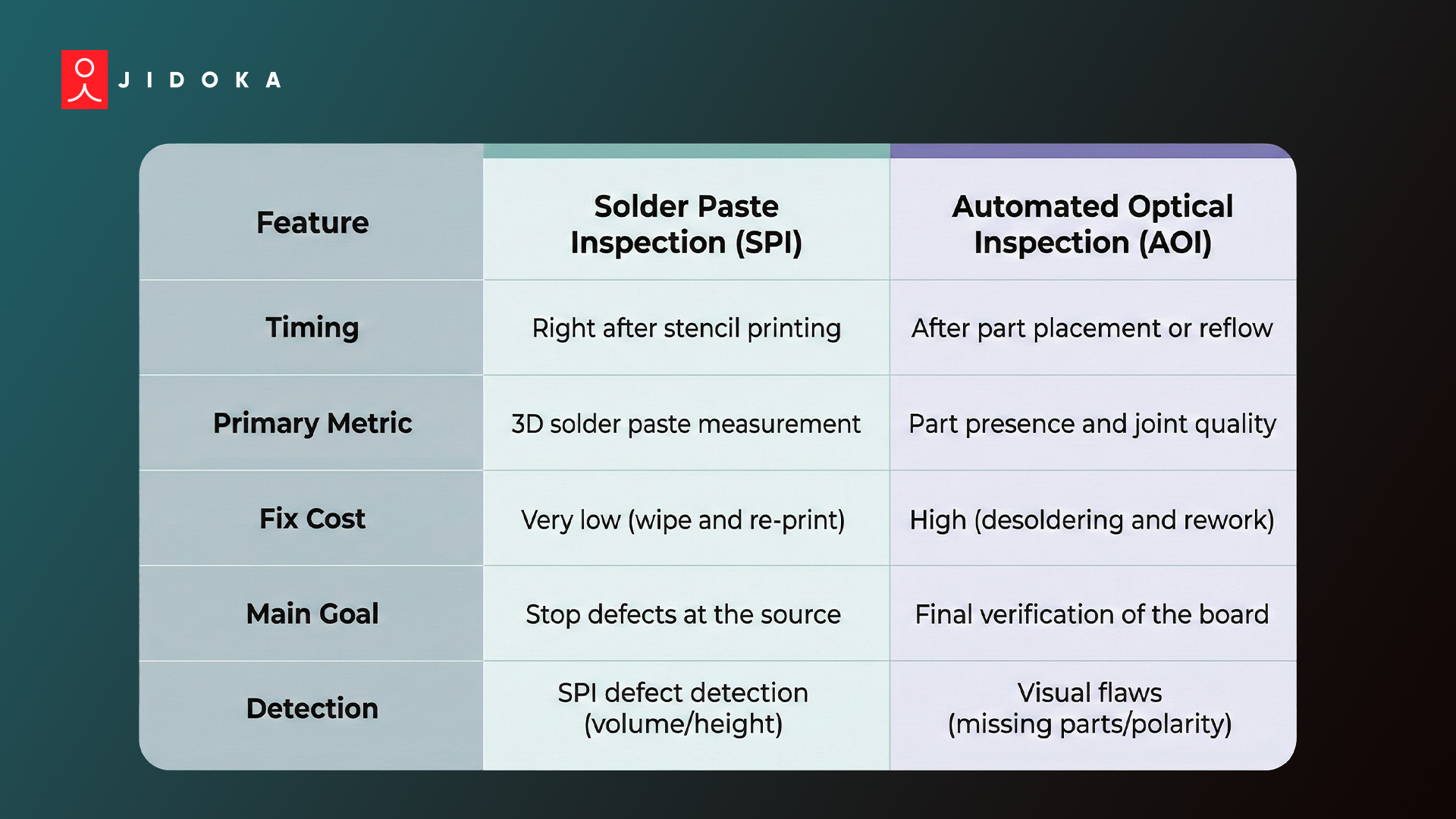
Esta tabla muestra por qué la inspección de la pasta de soldadura es una decisión inteligente. Si el AOI detecta un cortocircuito más adelante, puede consultar los datos del SPI. Esto le ayudará a comprobar si el problema se debe a una mala calidad de impresión con plantillas.
La conexión de estas máquinas crea un bucle de detección de defectos en tiempo real. Esta conexión le ayuda a encontrar la causa principal de cualquier fallo. Al combinar la inspección con pasta de soldadura y el AOI, se asegura de que cada placa sea perfecta.
Ahora, veamos cómo puede mejorar su proceso de impresión para evitar estos defectos por completo.
Optimización del proceso de impresión de plantillas
La prevención ahorra más dinero que la detección. Lo ideal es detener los defectos antes de que se produzcan para mantener limpios los informes de inspección de la pasta de soldadura.
Concéntrese en estas cuatro áreas para mejorar la calidad de impresión de su plantilla:
1. Diseño de plantilla: Utilice plantillas cortadas con láser con un nanorrevestimiento. La verificación de la apertura de la plantilla debe mostrar las aperturas 10— 20% más pequeño que las almohadillas. Esto ayuda a evitar que la pasta de soldadura se acumule en las piezas pequeñas.
2. Parámetros de la espátula: Establece tu velocidad entre 20—40 mm/segundo. Si vas demasiado rápido, llegas a «alcanzar su punto máximo». Si aplicas demasiada presión, sacas la pasta de los agujeros, lo que arruina la medición de la altura de la pasta.
3. Control ambiental: La pasta de soldadura es sensible. Mantenga la planta de su fábrica en 20-25 °C. La humedad debe permanecer por debajo del 60%. La alta humedad hace que la pasta se hunda, lo que perjudica la calidad del ensamblaje de la PCB.
4. Mantenimiento regular: Usa un limpiador automático de plantillas cada pocas impresiones. Los orificios obstruidos son el principal motivo de las alarmas de detección de defectos del SPI. Las plantillas limpias garantizan una inspección perfecta del volumen de pasta en todo momento.
La gestión de estos pasos hace que el ensamblaje de SMT sea mucho más fluido. Garantiza que la medición de la pasta de soldadura 3D se mantenga dentro de los límites correctos. Ahora veamos cómo Jidoka Tech usa la IA para hacer que todo este proceso sea aún más inteligente.
Implementación de la inspección inteligente de la pasta de soldadura con Jidoka Tech
Para las plantas que tienen una gran demanda, Tecnología Jidoka ofrece un sistema de inspección impulsado por IA que funciona bajo presión. Su equipo alinea las cámaras y la iluminación para que el sistema funcione en todos los turnos.
Las plantas que utilizan esta configuración reportan resultados consistentes incluso en Más de 12 000 piezas por minuto y 300 millones de inspecciones diarias. Jidoka combina dos herramientas para ir más allá de los controles estándar.
1. BRÚJULA alcances Precisión superior al 99,8% revisando los marcos en menos de 10 ms. Maneja fácilmente los metales reflectantes y las partes texturizadas.
2. NAGARE vías 100% de los pasos de ensamblaje para marcar las piezas faltantes o las secuencias incorrectas. Esto le ayuda a reducir el retrabajo en 20— 35%.
Al funcionar en unidades periféricas locales, este sistema de IA de inspección en línea evita demoras y mantiene los datos de inspección de la pasta de soldadura precisos en tiempo real. Reserva hoy mismo una consultoría con Jidoka Tech para ver cómo nuestra detección de defectos en tiempo real puede transformar su línea de producción.
Conclusión: el camino hacia una fabricación sin defectos
La pasta de soldadura es el pegamento de todos los dispositivos electrónicos. Cuando la inspección de la pasta de soldadura falla, surgen problemas ocultos, como uniones débiles y cortocircuitos irregulares. Los errores no detectados provocan fallos de campo, costosas retiradas del mercado y un deterioro de la reputación de la marca. Un lote defectuoso puede mermar sus ganancias y detener su crecimiento.
No permita que la mala calidad de la impresión de plantillas perjudique su éxito. Tecnología Jidoka proporciona la solución con un sistema de inspección impulsado por IA que detecta los errores antes de que salgan de fábrica.
Proteja su hardware y a sus clientes con una detección de defectos en tiempo real que funciona. Conéctese hoy mismo con Jidoka Tech.
Preguntas frecuentes
1. ¿Puede SPI detectar defectos en placas multicapa?
No, la inspección de la pasta de soldadura solo comprueba la superficie. Para detectar defectos internos o juntas ocultas, necesita una inspección por rayos X automatizada. Sin embargo, la detección de defectos mediante SPI garantiza que la calidad de impresión de las plantillas sea perfecta incluso antes de que estas capas se ensamblen en el producto final.
2. ¿Es necesaria la SPI 3D para los componentes de gran tamaño?
Sí. Incluso con piezas grandes, la medición de la pasta de soldadura en 3D es vital. Realiza un seguimiento de la altura y el volumen de la pasta para evitar que las articulaciones se debiliten. Este nivel de detección de defectos en tiempo real hace que su ensamblaje SMT sea confiable y mantiene una alta calidad de ensamblaje de PCB.
3. ¿Con qué frecuencia debo calibrar el sistema SPI?
La mayoría de los sistemas realizan una autocomprobación al inicio. Sin embargo, debe utilizar un placa maestra certificada semanalmente. Esto garantiza que la medición de la pasta de soldadura 3D se mantenga precisa, especialmente cuando los cambios de temperatura o humedad afectan a la calidad general de la impresión con plantillas.
4. ¿El SPI ayuda a verificar la apertura de la plantilla?
Absolutamente. Al controlar si hay «saltos» o puntos faltantes, el sistema proporciona una verificación constante de la apertura de la plantilla. Le avisa de inmediato si los orificios están obstruidos. Esta inspección automatizada del volumen de pasta detiene las fallas en el ensamblaje de los SMT en su origen antes de que se vuelvan costosas.
5. ¿Cómo evita el SPI la formación de puentes entre la pasta de soldadura?
El sistema utiliza la medición 3D de la pasta de soldadura para identificar cuándo la pasta se extiende entre las almohadillas. Al detectar al instante la pasta de soldadura que forma un puente, se borra automáticamente la plantilla. Esto mantiene alta la calidad del ensamblaje de su PCB y protege su línea de ensamblaje SMT.