Les défauts détectés à la fin d'une chaîne de production coûtent 100 fois plus cher à réparer que ceux détectés au début. Pourtant, de nombreuses usines se trompent encore lors de l'inspection des circuits imprimés. Ils considèrent les contrôles de qualité comme des événements isolés plutôt que comme un système cohérent. Cette approche consomme de l'argent. Une véritable efficacité passe par un bilan de santé continu à chaque étape.
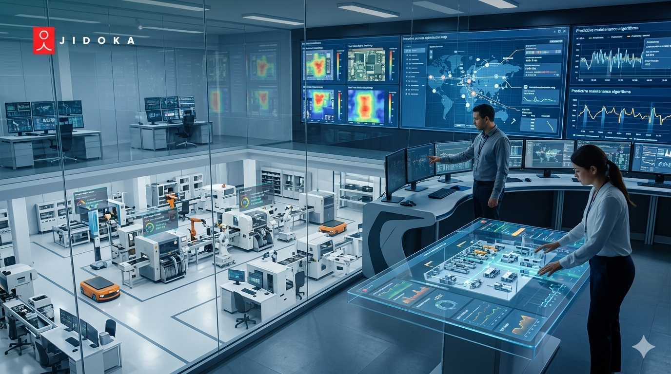
Ce guide vous guide à travers un cycle de vie en 7 étapes pour 2025. Nous allons au-delà des méthodes d'inspection de base des PCB et montrons comment l'inspection optique automatisée s'intègre dans un écosystème intelligent. Vous verrez comment fonctionne un AI Suit, comme celui de Jidoka, connecte ces étapes pour détecter rapidement les erreurs.
Réparons votre processus et l'inspection de votre circuit imprimé principal dès aujourd'hui.
Étape 1 : Traçabilité entrante et vérification des codes-barres
La plupart des lignes utilisent des lecteurs de codes-barres standard pour lire les codes gravés au laser, les codes QR ou Matrice de données estampes. Mais les scanners matériels échouent souvent dans des conditions réelles. Ils ont du mal à utiliser des masques de soudure brillants, des panneaux incurvés flexibles ou une gravure à faible contraste. Lorsqu'un scanner tombe en panne, la ligne s'arrête, ou pire encore, le tableau continue sans suivi.
La plateforme Kompass de Jidoka résout ce problème avec OCR piloté par l'IA. Il agit comme un œil humain mais traite les données instantanément.
- Lit les codes endommagés : L'IA déchiffre les codes partiellement masqués, rayés ou à faible contraste que les scanners matériels rejettent.
- Poignées Reflection : Il ignore les reflets du masque de soudure qui aveugle généralement les scanners laser traditionnels.
- Crée une identité : C'est ce que nous appelons le « certificat de naissance numérique ». Il enregistre immédiatement le tableau pour garantir une traçabilité à 100 %.
Sans cette étape, précise Détection des défauts des PCB devient impossible plus tard car vous n'avez aucune trace de l'origine du tableau.
Une fois la carte identifiée et enregistrée, nous passons à l'étape où se produisent la majorité des erreurs de fabrication.
Étape 2 : Inspection de la pâte à souder (SPI)
L'inspection de la pâte à souder (SPI) constitue la première barrière défensive lors de l'inspection des circuits imprimés. Des caméras 3D mesurent le volume, la surface et la hauteur des dépôts de pâte. Cela va au-delà de la simple imagerie 2D.
Le système garantit que l'imprimante dépose suffisamment de pâte pour former un joint solide, mais pas au point de provoquer des ponts. L'inspection fiable des circuits imprimés dépend de ces données volumétriques.
- La règle des 70 % : Les données du secteur confirment qu'environ 70 % de tous les défauts identifiés lors des pratiques de contrôle qualité des PCB remontent à l'impression.
- Le volume compte : Une image 2D plate peut montrer de la colle sur le tampon, mais une mesure 3D révèle si le dépôt est trop fin (provoquant des ouvertures) ou trop épais (provoquant des courts-circuits).
- Contrôle des coûts : C'est le point le moins cher pour corriger une erreur. Si l'inspection des circuits imprimés détecte une carte ici, vous la lavez et vous la réimprimez pour quelques centimes.
Permettre à une carte mal imprimée d'avancer garantit des retouches coûteuses par la suite.
Étape 3 : AOI de pré-refusion (placement des composants)
Caméras haute vitesse scannez le tableau immédiatement après que la machine pick-and-place ait terminé sa tâche. Cette forme d'inspection optique automatisée permet de vérifier la disposition physique des pièces avant leur entrée dans le four. Le système vérifie trois critères spécifiques :
- Présence : Le composant se trouve-t-il réellement sur la carte ?
- Polarité : La puce pique-t-elle correctement ?
- Alignement : La pièce repose-t-elle bien sur les coussinets ?
À ce stade, l'inspection AOI des PCB déclenche historiquement des taux de fausses alertes élevés. Les machines traditionnelles signalent chaque petit biais comme un défaut. Cependant, les modèles d'apprentissage profond de Jidoka comprennent la physique. L'IA sait qu'un condensateur légèrement incliné « s'autocorrige » souvent dans le four en raison de la tension superficielle de la soudure fondue.
Les techniques d'inspection des assemblages de cartes intelligentes font la distinction entre une erreur fatale et une erreur autocorrectrice. Cela permet d'éviter les arrêts de ligne inutiles tout en maintenant des normes strictes d'inspection des circuits imprimés.
Étape 4 : AOI post-refusion (The Critical Quality Gate)
Les opérateurs s'appuient sur cette étape pour détecter les erreurs de fabrication les plus courantes. Inspection optique automatisée avancée examine les joints de soudure finis pour signaler des modes de défaillance spécifiques tels que les courts-circuits (ponts de soudure), les ouvertures (tombstoning) et les vides (air emprisonné).
Les méthodes d'inspection standard des PCB échouent souvent ici car elles utilisent des caméras 2D. Une image 2D voit un joint brillant et le dépasse, mais un joint brillant peut toujours ne pas être connecté. L'inspection AOI moderne pour les PCB utilise Lumière structurée 3D pour mesurer la hauteur et la pente du filet de soudure.
Cela prouve que l'articulation a le bon »ménisque« forme et résistance mécanique. L'inspection de haute qualité des circuits imprimés exige cette perception de la profondeur pour garantir la fiabilité.
Une inspection efficace des circuits imprimés à ce stade empêche la détection des défauts des PCB sur le terrain, là où cela coûte le plus cher.
Étape 5 : Inspection par rayons X automatisée (AXI)
Les caméras optiques heurtent un mur lorsque le joint de soudure se trouve directement sous le corps du composant. Inspection par rayons X automatisée (AXI) résout ce problème en voyant à travers l'emballage. Elle reste la seule option viable pour les techniques d'inspection des assemblages de cartes impliquant des pièces à haute densité.
- Composantes cibles : Vous avez besoin de X-Ray pour Tableaux à grilles à billes (BGA) et Chip Scale Packages (CSP) où les connexions sont prises en sandwich entre la puce et la carte.
- Vices cachés : AXI détecte des défauts liés à la « tête dans l'oreiller », dans lesquels la bille de soudure repose sur la pastille mais ne fusionne pas. L'inspection visuelle des circuits imprimés passe à côté de cette étape 100 % du temps.
- Conformité : Les secteurs critiques pour la sécurité tels que automobile et l'aérospatiale mandatent X-Ray pour garantir l'intégrité structurale interne.
La détection des défauts des PCB reste incomplète si l'on ne regarde pas à l'intérieur des joints.
Une fois que la structure physique passe les rayons X, vous devez vérifier que la carte fonctionne réellement électriquement.
Étape 6 : Tests fonctionnels et électriques (TIC)
Après l'inspection optique automatisée et le nettoyage visuel de la carte par rayons X, le processus passe à Tests en circuit (ICT). C'est ce que l'on appelle souvent le test du « lit des ongles ». Pour les petits lots, les fabricants utilisent un système Flying Probe.
Les sondes entrent en contact physique avec des points de test spécifiques sur le circuit imprimé. Ils envoient des signaux électriques à travers le circuit pour mesurer les niveaux de résistance, de capacité et de tension.
- Vérification logique : Cette étape permet de vérifier que la carte exécute les fonctions logiques prévues.
- Défauts cachés : Il détecte les circuits ouverts ou les courts-circuits manqués par les caméras d'inspection des circuits imprimés, tels que les fractures de la racine des cheveux.
- Validation finale : Cette vérification électrique constitue la preuve ultime de vos pratiques de contrôle qualité des PCB.
CirL'inspection de la carte de circuit reste inachevée jusqu'à ce que vous confirmiez que le courant circule correctement.
Étape 7 : La « boucle dorée » (vérification assistée par IA)
Jidoka transforme cette vulnérabilité en utilisant inspection optique automatisée des PCB couplé à l'IA. C'est ce que nous appelons HILDA (Algorithmes conçus par l'humain). Lorsqu'une machine signale un défaut potentiel, l'IA agit comme un »Co-pilote.« Il présente l'image à l'opérateur avec un score de probabilité.
Surtout, le système apprend de la décision de l'homme. Si l'opérateur annule l'IA, le modèle est mis à jour instantanément. Cela crée une « boucle dorée » qui s'améliore d'elle-même. L'IA devient plus intelligente à chaque changement. Cela réduit considérablement les fausses alarmes lors de la détection des défauts des circuits imprimés et garantit que l'inspection des circuits imprimés reste précise au fil du temps.
Déploiement de la « combinaison IA » Jidoka tout au long du cycle de vie du SMT
Technologie Jidoka résout ce problème en créant un système d'inspection alimenté par l'IA qui fonctionne sous une pression de production réelle. Leur équipe aligne les caméras, l'éclairage et la synchronisation des automates pour que le système fonctionne sur tous les quarts de travail. Cela va au-delà des méthodes d'inspection standard des PCB.
Les usines utilisant la configuration de Jidoka enregistrent des performances constantes, même à des volumes extrêmement élevés, jusqu'à 300 millions d'inspections par jour. Cette robustesse provient de la combinaison de deux systèmes principaux qui étendent les capacités d'inspection des circuits imprimés :
1. KOMPASS : Inspecteur de haute précision
boussole alimente la logique de détection des défauts. Il atteint une précision de plus de 99,8 % sur les lignes en temps réel et passe en revue chaque image en moins de 10 ms.
- Adaptabilité : Il apprend de nouvelles variantes avec 60 à 70 % d'échantillons en moins que les modèles traditionnels.
- Maîtrise de la surface : Le système gère facilement les métaux réfléchissants et les pièces texturées. Il est donc idéal pour l'inspection des circuits imprimés, où les joints de soudure brillants et les traces de cuivre perturbent les caméras standard.
- Cohérence : KOMPASS prend en charge les déploiements où la cohérence visuelle est la plus importante.
2. NAGARE : Analyste des processus et de l'assemblage
Pendant que Kompass vérifie la pièce, Nagaré vérifie le processus. Il suit 100 % des étapes d'assemblage à l'aide de caméras existantes pour agir en tant qu' « intégrateur ».
- Logique en temps réel : Il signale instantanément les parties manquantes ou les séquences erronées.
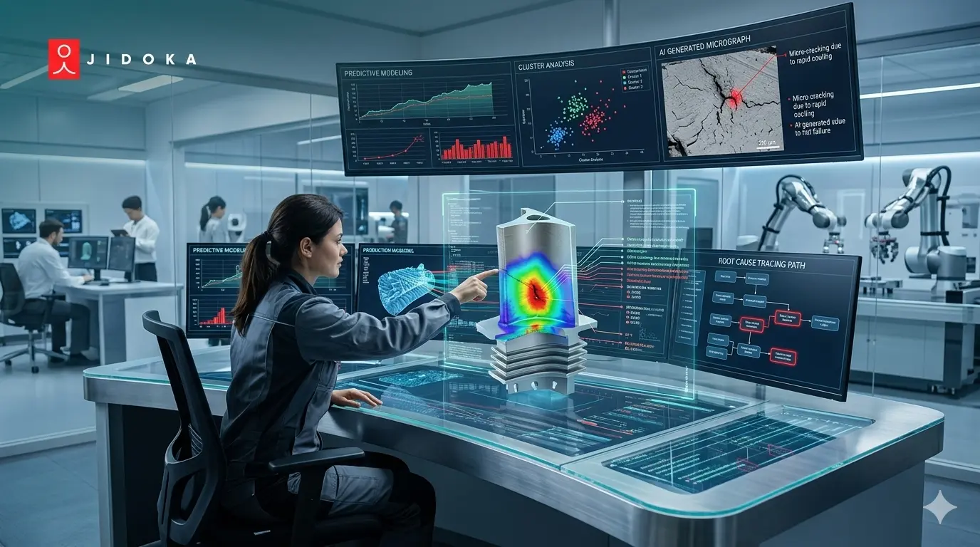
- Analyse des causes profondes : Si l'inspection optique automatisée détecte un défaut, Nagare le retrace jusqu'à la source.
- Résultat : Les usines utilisant Nagare ont réduit les retouches en De 20 à 35 % en renforçant les contrôles des stations et l'automatisation des inspections visuelles.
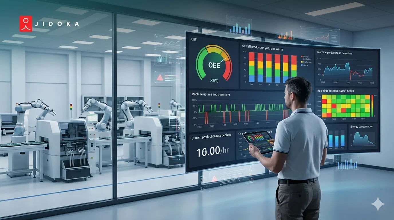
Jidoka gère cette suite complète d'inspection des circuits imprimés sur des unités périphériques locales afin d'éviter les retards liés au cloud. Cela garantit que vos pratiques de contrôle qualité des PCB restent rapides, sécurisées et unifiées sur un tableau de bord unique.
Conclusion
L'inspection de circuits imprimés fragmentés ressemble à combattre un incendie avec un pistolet à eau. Les machines déconnectées et les opérateurs fatigués laissent passer les défauts, tandis que les anciens systèmes d'inspection optique automatisés bloquent votre ligne en déclenchant de fausses alarmes.
Un seul défaut échappé réduit votre marge de profit. Pire encore, l'expédition de cartons défectueux déclenche des rappels et détruit la confiance des clients. Vous ne pouvez pas vous permettre un « angle mort » en 2025.
Jidoka Technologies arrête cette hémorragie. Nous installons un « AI Suit » unifié qui connecte l'ensemble de votre ligne. En reliant la détection de l'impression au test final, boussole et Nagaré détecter les erreurs à la source.
Êtes-vous prêt à combler les lacunes ? Auditez votre processus avec Jidoka dès aujourd'hui.
FAQs
1. Quelle est l'étape la plus critique de l'inspection des circuits imprimés ?
L'inspection de la pâte à souder (SPI) est vitale car 70 % des défauts commencent ici. La détection précoce des erreurs permet d'optimiser les coûts d'inspection des circuits imprimés. Si vous détectez des défauts maintenant, vous les corrigez à moindre coût. Attendre les étapes ultérieures rend la détection des défauts des PCB coûteuse. Prioriser le SPI améliore les pratiques globales de contrôle qualité des PCB et garantit des techniques d'inspection fiables des assemblages de cartes.
2. Comment la combinaison IA de Jidoka réduit-elle les faux positifs ?
Jidoka utilise HILDA pour affiner l'inspection optique automatisée. Le système apprend à partir des commentaires des opérateurs dans le cadre d'une « boucle dorée ». Ce processus permet de distinguer les erreurs réelles des ombres inoffensives, améliorant ainsi la précision de détection des défauts des PCB. Cela empêche l'inspection AOI des PCB de détecter de bonnes cartes, garantissant ainsi à votre équipe de se concentrer uniquement sur les véritables problèmes.
3. Jidoka peut-il s'intégrer à mes machines existantes (par exemple, Koh Young, Omron) ?
Oui, Jidoka agit en tant qu'intégrateur indépendant du matériel. Vous conservez vos méthodes et machines d'inspection des PCB actuelles. Nous superposons simplement notre « AI Suit » pour unifier les données de marques telles que Koh Young. Cela connecte vos systèmes d'inspection optique automatisés à un seul tableau de bord, améliorant ainsi les capacités d'inspection de vos circuits imprimés sans remplacer du matériel coûteux.
4. Pourquoi les rayons X (AXI) deviennent-ils obligatoires en 2025 ?
La miniaturisation est à l'origine de ce changement. Les composants tels que les BGA masquent les joints lors de l'inspection optique automatique standard des PCB. La radiographie reste le seul moyen de voir en dessous de ces parties. Il est essentiel pour vérifier l'intégrité structurale lorsque les techniques d'inspection des assemblages de cartes optiques échouent. L'inspection avancée des circuits imprimés nécessite AXI pour garantir l'absence de défauts.