
Electronics makers face a big problem. Many flaws stay hidden. You cannot see what happens under a chip with your eyes. This makes x-ray solder joint inspection a necessity. High quality x-ray solder joint inspection catches 99% of errors.
It simplifies BGA defect detection by looking through parts using automated X-ray inspection. You also get clear solder joint void analysis to stop heat buildup. This tech keeps your boards running. It prevents returns. You need it for high density circuits.
Solder Joint Defects: The Critical Five
You must know what you look for before starting. Solder defects hide inside high-density packages where your eyes cannot see. Identifying these five major flaws through x-ray solder joint inspection saves you from expensive rework.
1. Voids—The Most Common Hidden Defect
Voids are tiny air pockets trapped inside solder. They look like light spots in an X-ray because air has a lower density than metal. In 2026, manufacturers will use solder joint void analysis to measure these gaps.
While tiny bubbles are normal, gaps covering over 25% of the joint area cause trouble. They block heat, leading to overheating. Regular x-ray solder joint inspection helps you spot these solder joint voids before they weaken the bond.
2. Solder Bridges—Unwanted Electrical Connections
A bridge happens when solder spills over and connects two pads. BGA defect detection routines flag solder bridges as dark, messy blobs. These solder bridges cause shorts that fry components instantly. Since you cannot see under a BGA chip, x-ray solder joint inspection is your only way to find these hidden PCB defects.
3. Open Circuits—The Complete Connection Failure
An open circuit failure means the electrical path is broken. X-ray images show these as missing solder or a gap between the ball and pad. High-quality x-ray solder joint inspection uses angled views to confirm the break. Using non-destructive testing ensures you find these without breaking the board.
4. Shorts and Electrical Bridging
Shorts create low-resistance paths that draw too much current. x-ray solder joint inspection reveals these internal failures. Using BGA defect detection prevents these failures from reaching customers, supporting solder joint quality control.
5. Head-in-Pillow Defects—The Deceptive Failure
The head-in-pillow defect passes initial tests but fails when the board flexes. A detailed solder joint void analysis often reveals the subtle "waist" shape. Consistent x-ray solder joint inspection catches this head-in-pillow defect, ensuring a strong bond.
Knowing these flaws helps you choose the right tools to see them.
How X-Ray Solder Joint Inspection Works: From Imaging to Analysis
You need a way to look through metal and plastic without damaging the board. This is where x-ray solder joint inspection excels. It uses radiation to create a density map of your assembly, making it easy to spot PCB defects that stay hidden from cameras.
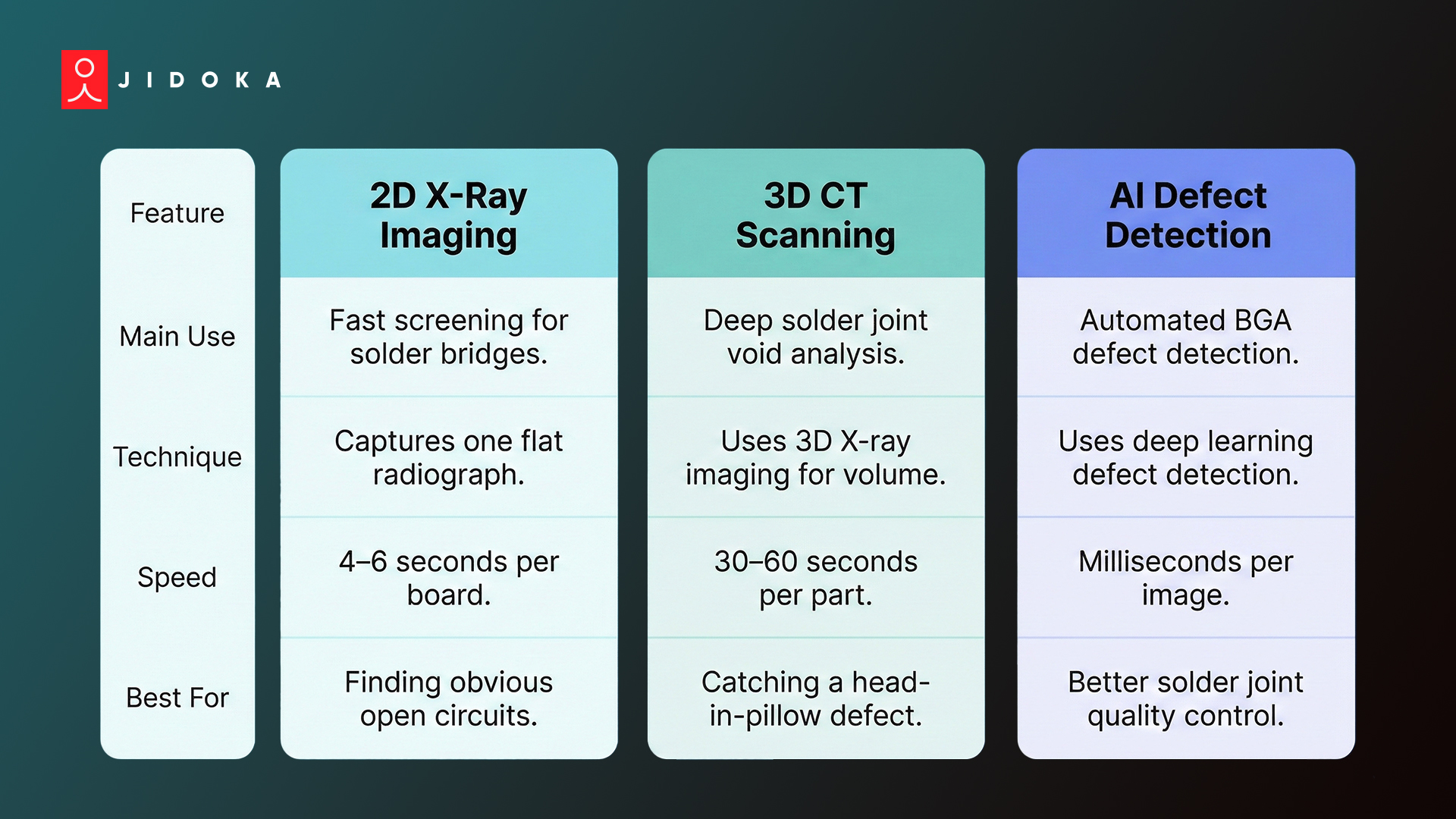
1. 2D X-Ray Imaging for Rapid Defect Detection
Most high-speed lines use 2D systems for quick checks. In these systems, an X-ray tube sends a beam through the board to a detector. Heavy materials like lead or tin block the beam and appear dark.
This makes x-ray solder joint inspection perfect for finding solder bridges or large solder joint voids. It is a fast form of automated X-ray inspection that keeps production moving.
2. 3D CT Scanning for Comprehensive Defect Visualization
When 2D is not enough, you use 3D Computed Tomography. This method rotates the X-ray source to take hundreds of photos from different angles. A computer then builds a 3D model of the joint.
This allows for precise solder joint void analysis because you can see the exact volume of the gap. It is the best tool for identifying a stubborn head-in-pillow defect or measuring internal open circuits.
3. AI and Deep Learning Transform Defect Classification
In 2026, deep learning defect detection will be the standard. Instead of a person squinting at a screen, AI models like ResNet-50 scan the images. These systems use automated X-ray inspection to find patterns that humans miss.
They offer better BGA defect detection by learning from thousands of images. This tech ensures your solder joint quality control stays consistent 24/7.
4. 3D X-ray imaging for Non-Destructive Testing
Using 3D X-ray imaging provides a complete view of the board's health. Because this is a form of non-destructive testing, you can inspect every unit without destroying a single one. This makes x-ray solder joint inspection the most reliable way to verify complex parts like BGAs and QFNs.
Detection Capabilities: What X-Ray Inspection Reveals vs. Misses
You need to know exactly what your tools can find to keep quality high. While x-ray solder joint inspection is powerful, it has specific limits you must manage. It remains the gold standard for checking hidden areas in BGAs and QFNs.
1. What X-Ray Inspection Detects with Precision
Your system finds internal PCB defects that other tools miss. High-quality x-ray solder joint inspection provides clear data on:
- Solder joint voids and their total volume.
- Solder bridges between tiny pads.
- Open circuits and missing solder balls.
- Head-in-pillow defect geometry using angled views.
- Broken wire bonds inside high-end chips.
Current automated X-ray inspection systems use solder joint void analysis to compare your boards against IPC-A-610 standards. For most products, voids covering more than 25% of a joint are a failure.
These measurements help you maintain strict solder joint quality control without slowing down your line.
2. The Head-in-Pillow Challenge—Detection Without Certainty
Finding a head-in-pillow defect is still the biggest challenge. A standard top-down X-ray might show a perfect circle, even if the ball hasn't fused to the paste. To solve this, you need 3D X-ray imaging or oblique views.
These methods look at the joint from the side to see the "waist" where the two metals should have merged. Even with deep learning defect detection, some cases require a manual double-check to be 100% sure.
3. Process Intelligence from Defect Patterns
Your x-ray solder joint inspection data tells a story about your assembly line. If you see solder bridges in the same spot every time, your stencil is likely dirty. If solder joint voids increase, your reflow oven might need a new profile. This data turns non-destructive testing into a tool for continuous improvement.
Reliable detection depends on following the right rules and industry benchmarks.
Industry Standards and Compliance Framework for Solder Inspection
You must follow global rules to ensure your boards are safe for use. The electronics world relies on specific benchmarks to decide if a joint is "good" or "bad." Using x-ray solder joint inspection allows you to meet these strict requirements without guessing.
1. IPC Standards Define Defect Thresholds
The IPC-A-610J (released in 2024) is the main guide for assembly quality. It groups products into three classes:
- Class 1: General electronics like toys or basic gadgets.
- Class 2: Dedicated service tools like laptops or TVs where long life matters.
- Class 3: High-performance systems like medical implants or flight controls where failure is not an option.
Standard x-ray solder joint inspection helps you categorize PCB defects based on these classes. For example, a tiny gap might pass in Class 1 but fail in Class 3. Most pros use solder joint void analysis to ensure that voids do not exceed 25% of the total area, which is a common limit for reliable BGA defect detection.
2. Application-Specific Standards
Different industries have extra rules. Automotive makers often demand tighter solder joint quality control, sometimes capping voids at 20%. Aerospace firms might require zero open circuits and high-resolution BGA defect detection.
By using x-ray solder joint inspection, you create a digital record that proves your boards meet these high bars. 3D X-ray imaging is often needed for these high-reliability parts to catch a head-in-pillow defect.
3. Documentation and Traceability
Modern systems record every flaw they find. Every time you perform BGA defect detection, the software saves the image. This data is vital for "traceability." If a part fails, you look back at the solder joint void analysis from the day it was made.
X-ray solder joint inspection provides the non-destructive testing data required for audits. Using deep learning defect detection ensures your records are accurate and free of human error.
Following these standards keeps your quality consistent and your customers happy.
How Jidoka Tech Delivers 99.8% Accuracy for High-Speed X-Ray Solder Inspection
Jidoka Tech builds an AI "suit" for total quality control. Their team aligns cameras and PLC timing so your x-ray solder joint inspection works perfectly.
- KOMPASS: Hits 99.8%+ accuracy for BGA defect detection. It scans frames in 10ms to find solder joint voids using deep learning defect detection.
- NAGARE: Tracks every assembly step to flag open circuits or solder bridges.
This automated X-ray inspection performs non-destructive testing on your PCB defects. It uses solder joint void analysis and 3D X-ray imaging to catch a head-in-pillow defect instantly, ensuring high solder joint quality control.
Contact Jidoka Technologies today to secure your production line with 99.9% accuracy.
Conclusion
Reliable x-ray solder joint inspection is vital for finding hidden connections in today’s dense electronics. Without rigorous x-ray solder joint inspection, PCB defects like solder joint voids go unnoticed. Undetected failures in EV power systems or 6G infrastructure lead to catastrophic recalls and ruined reputations.
Avoid these disasters by using Jidoka Technologies. Their AI-driven solder joint void analysis and KOMPASS system deliver 99.9% accuracy for BGA defect detection. Jidoka provides the real-time solder joint quality control you need to stop defects before they reach the field.
Talk to Jidoka’s experts to automate your quality control with 99.9% detection accuracy.
FAQs
1. What is the difference between 2D and 3D x-ray solder joint inspection?
2D systems provide rapid, top-down radiographs ideal for spotting solder bridges and large solder joint voids. However, 3D X-ray imaging captures volumetric data, allowing for deeper solder joint void analysis and the identification of hidden open circuits in stacked packages.
2. Can automated X-ray inspection catch every head-in-pillow defect?
Standard top-down views often miss this flaw. High-end automated X-ray inspection uses oblique angles and deep learning defect detection to identify the unique "waist" of a head-in-pillow defect. This ensures superior solder joint quality control compared to manual checks.
3. What is a safe level for solder joint voids?
Per IPC-A-610J standards, solder joint voids should not exceed 25% of the total area. High-reliability sectors use solder joint void analysis to enforce stricter 20% limits. Frequent x-ray solder joint inspection prevents these PCB defects from compromising thermal performance.
4. Does x-ray solder joint inspection damage the PCB?
No, this is a form of non-destructive testing. The radiation levels used in automated X-ray inspection are safe for components while providing clear views of internal PCB defects. It is the most reliable method for verifying solder joint quality control.
5. How does AI help with BGA defect detection?
Deep learning defect detection trains on millions of images to instantly recognize solder bridges and open circuits. This technology removes human bias from BGA defect detection, accelerating your x-ray solder joint inspection workflow while maintaining a 99.9% accuracy rate.