38.43 million electronic units were recalled globally in 2023 because legacy inspection missed underlying defects, generating $5.5 billion in warranty claims in 2022 alone. Solder paste defects account for 35% of all SMT assembly failures and consistently surface at the customer, not the inspection station (ltcircuit.com, 2024).
Electronics manufacturing quality degrades the moment inspection becomes a bottleneck. The structural fix is AI vision that operates at production speed, not sampling speed. This guide breaks down why legacy inspection fails at volume, what AI vision does differently, and how KOMPASS and NAGARE deploy without disrupting active electronics lines.
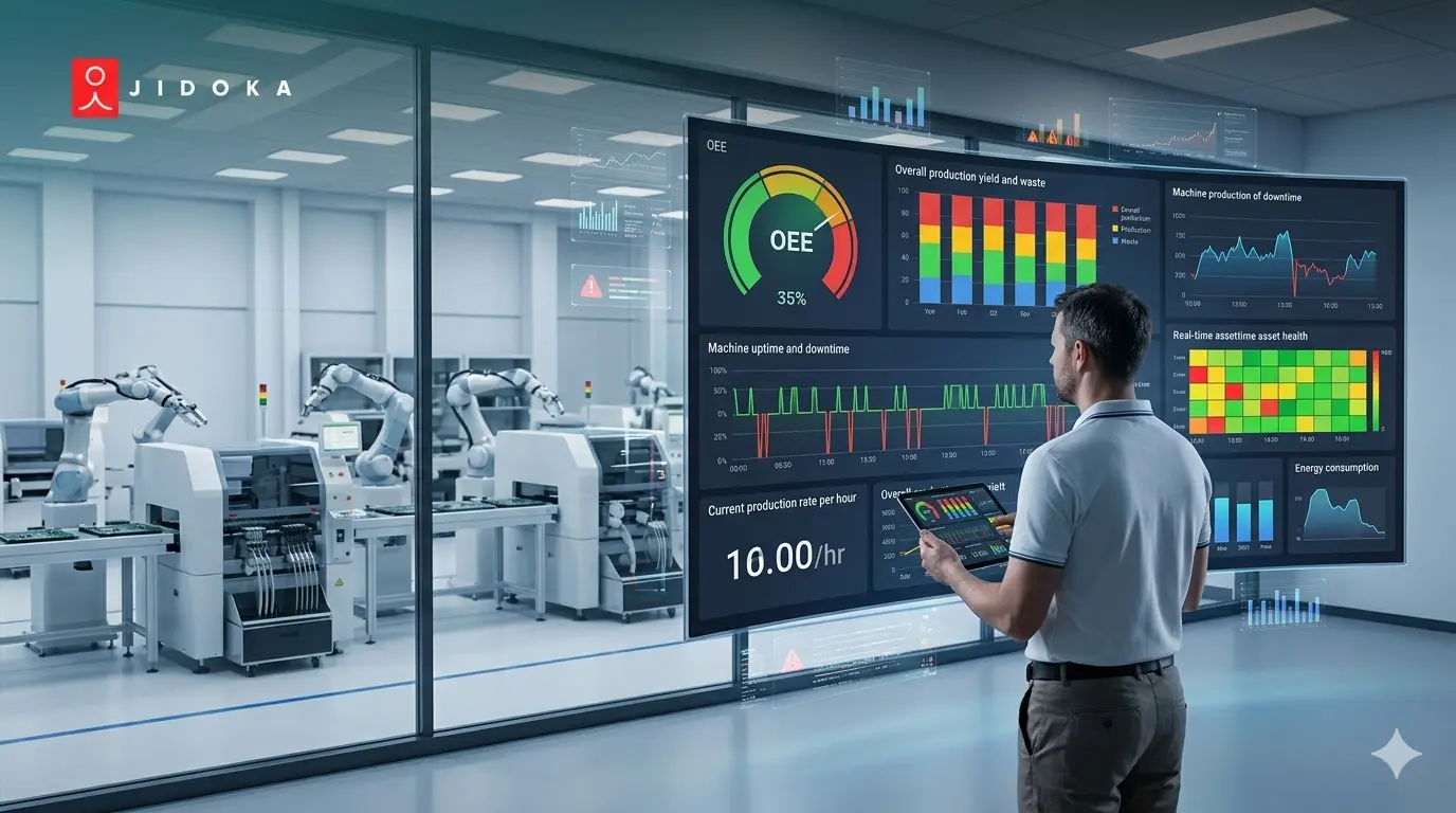
Key Takeaway: Electronics manufacturers don't face a quality versus throughput trade-off. They face an inspection architecture problem. Traditional automated optical inspection tops out at approximately 1,000 parts per minute, creating line bottlenecks. KOMPASS by Jidoka inspects at 12,000 PPM with 99.9% accuracy, eliminating the bottleneck entirely while maintaining full inline defect detection coverage on every unit.
What Does Electronics Manufacturing Quality Require That Traditional Inspection Cannot Deliver?
Electronics manufacturing quality at scale requires 100% inline inspection of solder joints, component placement, connector integrity, and assembly sequences with zero throughput reduction. Sampling-based audits and legacy automated optical inspection miss shift-level variation and the high-mix defect patterns that only emerge at full production volume.
The Throughput Ceiling of Rule-Based AOI
Traditional automated optical inspection tops out at approximately 1,000 parts per minute. Any electronics manufacturing quality line running above 3,000 PPM faces a structural choice: slow the line to match inspection speed, or run inspection as a partial sample and accept blind zones. Both outcomes produce escapes.
High false-positive rates compound the problem. When an inspection station flags 30% of units incorrectly, operators learn to override alerts. That override habit creates the gaps through which real defects travel undetected. The aggregate outcome is the 38.43 million unit recall figure: not a single catastrophic failure, but thousands of individual inspection escapes across global electronics production accuracy failures. See how Jidoka addresses this across the electronics industry with continuous verification.
What High-Mix SKU Changeover Does to Defect Profiles
Each product variant in a high-mix electronics line generates a distinct solder joint geometry, connector configuration, and defect signature. Rule-based AOI is configured against one reference state. When the line switches from variant 1 to variant 3, the inspection system is still looking for variant 1 defect patterns.
The result: pcb assembly quality monitoring that is accurate for the morning SKU becomes structurally blind to the afternoon SKU's specific failure modes. Terminal crack patterns change with connector type. Solder void geometry varies with pad density. A fixed-rule system requires manual reprogramming per changeover, which takes hours the production schedule does not have. Electronics assembly verification at this level needs adaptive AI, not static templates.
How Does an Electronics Quality Control System Using AI Differ From Rule-Based AOI?
An AI-powered inspection system uses deep learning to adapt defect detection per SKU, inspect every unit at full production speed, and trigger automatic rejection on defects. Legacy automated optical inspection uses fixed rules requiring manual reprogramming per changeover and cannot detect previously unseen defect types when product variants shift.
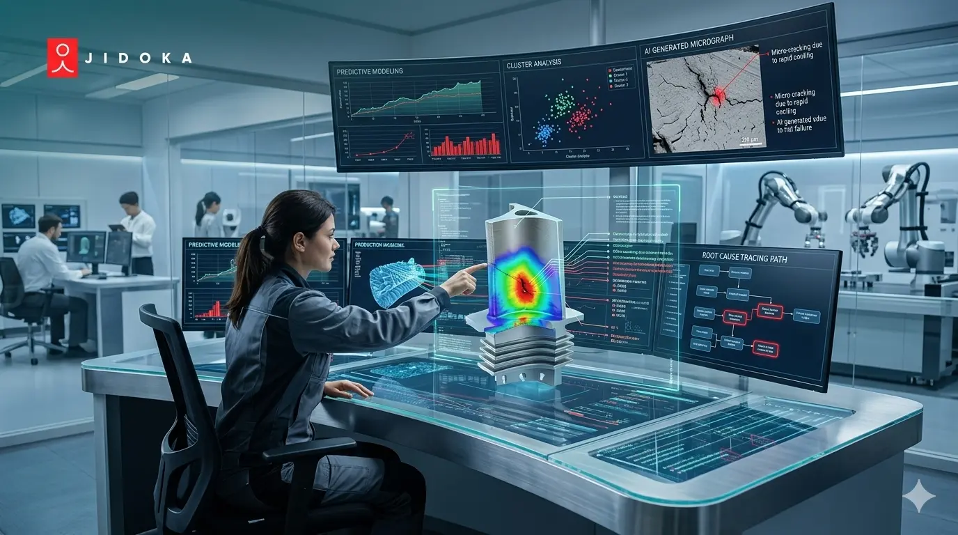
KOMPASS Architecture and the DOJO Self-Training Engine
KOMPASS processes images at the edge, on-premise, with multi-angle inspection and sub-10-millisecond classification per unit. The DOJO self-training workflow runs in four steps: define the part and label reference images; upload the image set (fewer than 10 good reference images required per part); train and validate the model; deploy to live production. No external ML engineers are needed at any stage.
The electronics quality control system outcomes from KOMPASS deployments: 99.9% defect detection accuracy, 40% reduction in false rejections, and 12,000 PPM throughput.
KOMPASS inspects what products look like. NAGARE monitors what operators do to create them. In electronics manufacturing quality control, that distinction is the difference between detecting a defect and preventing the next one. Inconsistent torquing sequences on PCB assemblies and telecom boards create micro-cracks invisible at inline inspection. Those micro-cracks generate field failures under thermal or mechanical stress, weeks or months after the product shipped.
NAGARE monitors torquing sequences in real time against the digital SOP, intercepting this failure mode before it compounds. Electronics manufacturers using NAGARE on assembly lines report a 20% reduction in defective units from process-origin errors and 100% process adherence via real-time operator guidance.
Which Defects in Circuit Assembly Quality Does AI Vision Catch That Sampling Misses?
AI vision in electronics manufacturing quality catches defect types invisible to rule-based systems: edge-case solder variations, early-stage connector corrosion, subtle casing deformities, and process-origin micro-cracks from incorrect torquing that only surface as field failures under thermal or mechanical stress after the product ships.
Solder and PCB Defects That Surface Downstream
Cold joints, solder voids, solder bridges, missing and misplaced components, and wrong polarity are circuit assembly quality failures that traditional AOI misses when board density increases or lighting conditions shift. Any of these reach the customer as a functional failure or a warranty return.
KOMPASS outcomes on PCB lines: 99% defect detection accuracy, 20% reduction in rework, 10% higher throughput. The 35% of SMT failures originating in solder paste defects (ltcircuit.com, 2024) are precisely the class of defects that smt inspection process systems running at sampling speed cannot reliably intercept before production advances.
Connector and Terminal Faults That Drive Warranty Claims
Terminal cracks at early formation stage, crimping inconsistency, corrosion, and moulding defects in connectors are the cumulative driver behind the $5.5 billion global warranty burden. These defects are electronics defect prevention failures: they originate at production and surface in the field, because sampling-based pcb assembly inspection lacks both the coverage and the sensitivity to catch them inline.
KOMPASS outcomes on connector lines: 15% reduction in warranty claims, 20% higher throughput versus manual inspection. Both metrics compound over a production year: fewer warranty returns reduce support cost; higher throughput increases revenue per machine-hour.
Process-Origin Defects That No Product Inspection Can Catch
Incorrect torquing sequences produce no visible surface artifact on the board. Product inspection systems have nothing to detect. No camera angle, no lighting configuration, no rule set changes that structural limitation. The only way to intercept this failure mode is process monitoring: NAGARE monitoring the torquing sequence against the digital SOP in real time as the operator executes each step.
This is the key differentiation argument for combining KOMPASS and NAGARE: electronics manufacturing quality has four defect categories, and the fourth one (process-origin failures) is structurally inaccessible to any product inspection architecture. Casing and cosmetic defects alone show a 12% inspection speed improvement with AI over manual methods.
How Does AI Improve Electronics Manufacturing Quality Without Slowing Throughput?
AI vision improves electronics manufacturing quality without adding inspection time by operating at 12,000 PPM inline, faster than most assembly lines run. Defect decisions happen in milliseconds with automatic rejection routing, creating no queue at the inspection station and no trade-off between coverage and line speed.
The Bottleneck Removal Economics
Conventional inspection runs below line speed. It creates a queue. The queue either slows the line or gets bypassed. Both outcomes reduce the effective quality gate to a fraction of production output. AI vision at 12,000 PPM runs above most electronics assembly line speeds. The inspection station is never the rate-limiting step.
The ROI model changes fundamentally when inspection is treated as a yield enabler rather than a compliance cost center. Every defect caught inline costs the reject price of one unit. Every defect that escapes inline and reaches the field costs warranty service, brand exposure, and potential recall. The math of electronics manufacturing quality improvement always favors prevention over recovery.
Jidoka Electronics ROI Data
Jidoka electronics deployments deliver $40,000 in annual savings per production line, an 18% boost in production efficiency, and a 22% reduction in defective units when KOMPASS and NAGARE run together. Positive ROI arrives within 8 to 14 months. These figures cover the product-detection gain from KOMPASS and the process-compliance gain from NAGARE as a combined system outcome, not as separate metrics from isolated deployments.
NAGARE's parallel impact: while KOMPASS removes product inspection bottlenecks, NAGARE removes process compliance bottlenecks by replacing manual supervisor rounds with continuous automated verification. Combined, the two systems deliver electronics assembly verification across both product quality and process quality dimensions simultaneously.
How Do Electronics Manufacturers Deploy AI for PCB Assembly Inspection on Active Lines?
Electronics manufacturers deploy AI for pcb assembly inspection without disruption by integrating KOMPASS with existing cameras, PLCs, and conveyor systems. The DOJO self-training engine trains SKU-specific inspection models in days, with live deployment achievable in 6 to 8 weeks alongside active production without stopping the line.
Hardware Integration and Infrastructure Compatibility
KOMPASS integrates with existing camera infrastructure. Where cameras are absent, Jidoka's modular vision hardware platforms (Tigris, Huron, Fujin) serve as drop-in inspection stations. NAGARE deploys on existing CCTV and shop-floor cameras, on-premise, with no cloud dependency. Both connect to PLCs for automated rejection triggering and to MES and ERP systems for full circuit assembly quality traceability.
This hardware-agnostic approach eliminates the capital barrier that makes traditional pcb assembly inspection upgrades difficult to justify. Existing infrastructure becomes the deployment substrate. The investment goes into the AI model and integration, not into replacing functional hardware. Jidoka's defect detection and assembly validation use cases cover the full deployment scope.
Timeline and the DOJO Training Process
From model training to live deployment, the typical timeline is 6 to 8 weeks. Quality engineers define parts, upload fewer than 10 reference images, validate model accuracy on test samples, and deploy without external ML engineers. The entire process runs within the quality team's existing capability.
Start the pilot on the line with the highest field return rate or rework cost, not the easiest station to integrate. The pilot data builds the business case for facility-wide rollout without requiring full capital commitment upfront. An electronics quality control system that proves ROI at the hardest station justifies every subsequent deployment.
How Jidoka Electronics Deployments Perform
KOMPASS and NAGARE together address both defect categories that conventional electronics manufacturing quality programs miss: product defects that AOI escapes at changeover or high density, and process-origin failures that no product inspection can detect.
- KOMPASS AI: 99.9% defect detection accuracy at 12,000 PPM. 40% fewer false rejections. 20% less rework on PCB and connector lines. [VERIFY: jidoka-tech.ai/products/kompass]
- NAGARE AI: 100% torquing sequence and assembly SOP verification. 20% reduction in defective units from process-origin errors.
- Combined: $40,000 annual savings per line, 18% production efficiency gain, 22% defect reduction, 8-14 month ROI.]
Book a deployment assessment to see how KOMPASS and NAGARE integrate with your electronics assembly line without halting active production.
Conclusion
Electronics manufacturing quality and throughput are not competing goals. Both are determined by whether inspection runs at line speed or creates a bottleneck. Every defect that clears AOI and reaches the field costs multiples more to resolve than one caught inline at the production point.
See how KOMPASS and NAGARE deliver 99.9% inspection accuracy at 12,000 PPM across electronics assembly lines at jidoka-tech.ai/industry/electronics.
Frequently Asked Questions
1. What is electronics manufacturing quality and why is it harder to maintain in high-mix production?
Electronics manufacturing quality means every unit meets exact specifications for solder integrity, component placement, connector reliability, and dimensional accuracy. High-mix production makes this harder because each product variant generates a distinct defect profile. Rule-based systems need manual reconfiguration per SKU, leaving inspection gaps at every changeover that only adaptive AI closes continuously.
2. How does an AI electronics quality control system differ from traditional automated optical inspection?
Traditional AOI uses fixed programming rules that fail when product variants or conditions change, and tops out at approximately 1,000 parts per minute. An AI electronics quality control system uses deep learning to adapt per SKU, inspect at 12,000 PPM, make real-time rejection decisions, and detect previously unseen defect types without manual reprogramming between production runs.
3. What specific defects does KOMPASS detect in PCB assembly inspection?
KOMPASS detects cold solder joints, solder bridges, insufficient solder, component misplacement, and wrong polarity in PCB assembly. For connector lines, it identifies terminal cracks, crimping defects, corrosion, and moulding defects. Electronics manufacturers using KOMPASS report 99% defect detection accuracy, 20% lower rework rates, and 15% fewer warranty claims from connection failures.
4. What role does NAGARE play in electronics manufacturing quality control?
NAGARE monitors operator actions, not just product appearance. In electronics manufacturing quality control, it verifies torquing sequences in real time against digital SOPs, preventing the process-origin micro-cracks that vision inspection cannot detect because no surface artifact exists at the point of creation. Manufacturers using NAGARE on electronics lines report a 20% reduction in defective units from process-origin errors.
5. What ROI do electronics manufacturers typically see from AI vision inspection systems?
Electronics manufacturers using Jidoka's KOMPASS report $40,000 in annual savings per production line, 18% boost in production efficiency, 15% reduction in warranty claims, and positive ROI within 8 to 14 months. The largest gains come from eliminating rework loops, reducing false rejections, and preventing the field failures that traditional AOI and manual inspection consistently miss.