











EDGE DEFECT & CHIPPING INSPECTION

Edge Chipping Inspection AI
to Catch Damage Around the Part

KOMPASS AI checks visible edge chipping, missing corners and breakouts on manufactured parts. Bring the critical edges into view, distinguish damage from the intended profile and flag affected units before assembly or packing makes another inspection harder.

Discuss Your Edge Inspection

Trusted by manufacturers to improve quality on the line

THE PROBLEM

A Good Top Surface Can Hide a Damaged Edge

Edge chipping often sits outside the view used to inspect the main surface. A broken corner, damaged rim or small breakout along a side can pass a face check and reach the next operation unseen.

The Critical Edge Faces Away From the Camera

A top view may miss damage on the lower rim or sidewall. Fixtures and handling can cover exactly the region that needs checking.

The Intended Profile Looks Like a Defect

Chamfers, radii, notches and normal cut texture change the outline. Inspection has to recognise the design before it can judge missing or excess material.

The Chip Is Found After the Part Is Installed

A damaged edge can affect appearance or interfere with the next operation. Once the part is assembled, isolating it may mean dismantling and rechecking the build.
The Solution

Inspect the Edges Your Acceptance Criteria Depend On

Our AI Product Inspection system, KOMPASS™, combines visual defect classification with modular vision hardware. The inspection is designed around the accessible edges, the intended profile and the smallest damage your process needs to reject.

Distinguish Local Damage From the Designed Edge

  • Train with acceptable chamfers, radii and normal manufacturing variation
  • Identify visible chips, missing corners and agreed breakout defects
  • Assess each critical region against the product's acceptance criteria
  • Validate borderline examples before the decision controls rejection
Intended profile
Represented in the good-part samples
Local damage
Assessed against your acceptance limits
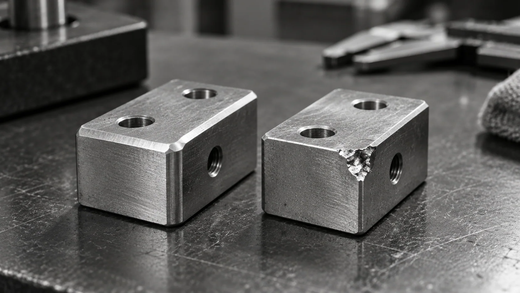
Conceptual illustration of an intact machined chamfer beside a chipped corner.
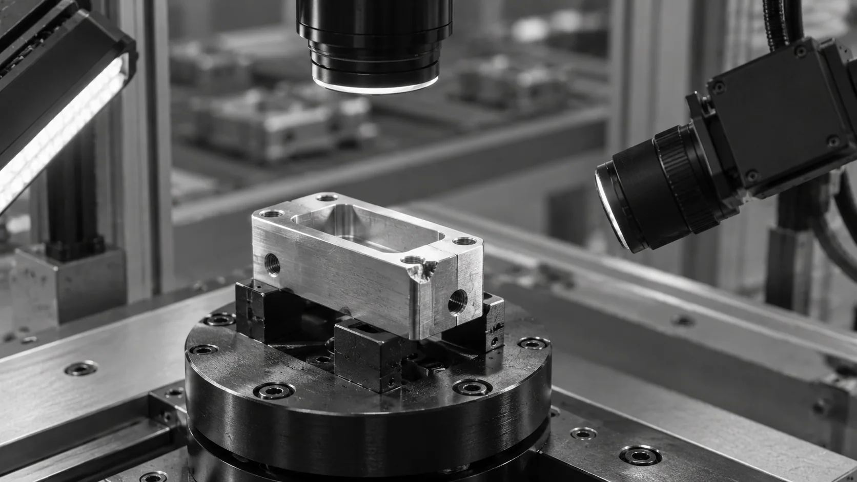
Conceptual illustration of overhead and angled cameras facing a chipped component in a fixture.

Bring the Required Perimeter Into View

  • Select face, side and angled views around the critical edges
  • Assess rotation, flipping or other handling where one view is insufficient
  • Connect the inspection decision to the configured reject or review response
  • Retain images to show the location and appearance of rejected damage
Critical views
Planned around the part and fixture
Defect location
Visible evidence for follow-up
HOW IT WORKS

Bring the Critical Edge Into View

An edge check needs a clear view of the region that matters. Plan the presentation, distinguish damage from intended geometry and keep the image with the inspection decision.

Highlight #1

Expose the Critical Edge

Plan camera views around the areas where damage matters. Check whether the fixture hides the lower rim, a sidewall or a corner, and whether the part needs to be turned.

Highlight #2

Judge the Damage in Context

The model uses production examples to distinguish the agreed defects from acceptable geometry and finish. A designed notch or chamfer belongs in the reference samples.

Highlight #3

Keep the Finding With the Decision

Connect the inspection result to the defined line response and retain the defect image. Quality teams can review where the damage occurred and whether the same location keeps appearing.

Connect With Us

Show us a chipped part, an acceptable edge and the tolerance that separates them. We will assess the views needed to make that decision repeatable.

Get In Touch

The Edge Needs Its Own Acceptance Decision

A method that works on a repeatable silhouette may be enough for one part. A complex edge with varying appearance needs a different combination of views and decision tools.

Inspection need
Manual inspection
Traditional machine vision
KOMPASS AI
Edges outside the top view
Inspector turns the part to inspect each region
Additional views or handling expose the required areas
Views and handling are selected for the critical perimeter
Designed features versus damage
Relies on knowledge of the drawing and visual standard
Effective for stable silhouettes and explicit geometric tolerances
Learns acceptable appearance alongside agreed defect examples
Evidence behind a rejection
Depends on the recording procedure
Can save images and measurement results
Retains visual defect evidence with the inspection result
First-Time-Right
Depends on consistent checks before assembly
Supports a defined edge checkpoint
Helps contain visible edge damage before the next operation

Frequently Asked Questions

What counts as edge chipping or another edge defect?

An edge defect is a departure from the accepted condition of the part's boundary. It can include a missing corner, a local breakout or another visible irregularity defined in your quality standard. Edge chipping detection focuses on unintended loss of material. The decision should account for size, location and the function of the affected region. Bring the drawing and representative parts to the review so the team can distinguish a cosmetic limit from a requirement that affects assembly or use.

How do you distinguish a chip from a chamfer or designed notch?

Chipped edge detection starts with a clear definition of the intended profile. Good samples should include the chamfers, radii, notches and normal cut texture that production is allowed to have. Chipping inspection then assesses departures from that accepted appearance. Include borderline rejects and accepted parts that look similar. If the decision depends on a measured geometric tolerance, specify the required measurement and reference so the imaging and calibration can be assessed alongside the visual classification.

Can one camera inspect the whole edge?

Only if its view exposes every region required by the acceptance standard. Edge quality inspection may need top, bottom and side views, or handling that rotates or flips the component. A fixture can hide an edge even when the camera has enough resolution to see the defect. Check the proposed presentation using damaged samples at each critical location. Coverage should describe the regions actually inspected, including any inaccessible area that needs a separate checkpoint.

Can the system inspect glass and ceramic components?

Glass edge inspection needs an imaging arrangement that manages transparency, reflections and the position of the damage. Ceramic inspection also depends on the component's finish, contrast, dimensions and presentation. Jidoka lists glass, ceramic and machined parts within this use-case scope, but each application needs sample testing. Include chips on different faces and corners, together with acceptable variations. The trial should establish visibility and detection limits for the actual parts instead of assuming one setup works across materials.

Can it check burrs at the same time?

Burr detection and broken edge detection concern different forms of damage. A burr adds unwanted material to the boundary, while a chip removes material. They can share an inspection station if its views and lighting expose both clearly. Keep the defect categories and acceptance criteria separate during validation. That makes it possible to review missed defects and false rejects for each task, and prevents a good overall result from hiding weak performance on one category.

Will the system measure chip depth or certify the edge geometry?

Edge profile inspection requires a defined reference and suitable measurement capability. A visible outline can show that material is missing without establishing the full depth of the break. If acceptance depends on depth, radius, angle or a calibrated dimensional limit, specify those requirements during feasibility. The team can then assess whether appropriate 3D sensing or another measurement method is needed. Visual classification alone should not be treated as a dimensional certificate or proof of internal integrity.

Is this also a wafer or semiconductor inspection solution?

Wafer edge inspection has specialised requirements for resolution, handling, cleanliness and defect classification. Those must be assessed for the particular process. The bearing video on this page demonstrates a multi-surface inspection approach and is not evidence of wafer capability. For electronics components, share the material, dimensions, critical edge regions and acceptance criteria with Jidoka. A feasibility study can establish whether the required views and detection performance are achievable for that specific component and production environment.

What should we measure during the trial?

Validate chip inspection with a labelled set covering the smallest rejectable damage, accepted edge variation and each important location on the part. Use samples that were not part of training and test the intended speed, fixtures and orientations. Record missed defects and good parts rejected separately. Also verify that the configured response acts on the correct unit. Together, those checks establish whether the complete station can support your quality decision under production conditions.

CONNECT WITH OUR EXPERTS

Show Us the Edge That Fails Your Quality Check

Share your damaged samples, accepted edge profile and required production rate. We will assess how to expose the critical regions and validate the decision before the part moves on.

Discuss Your Edge Inspection
Close video