%20How%20to%20Carry%20Out%20Circuit%20Board%20Inspection%20in%202025_.jpg)
Defects found at the end of a production line cost 100 times more to fix than those caught at the start. Yet, many factories still get circuit board inspection wrong. They treat quality checks as isolated events rather than a cohesive system. That approach burns money. True efficiency requires a continuous health check at every stage.
This guide walks you through a 7-step lifecycle for 2025. We move beyond basic PCB inspection methods and show how automated optical inspection integrates into a smart ecosystem. You will see how an AI Suit, like the one from Jidoka, connects these steps to catch errors early.
Let’s fix your process and master circuit board inspection today.
Step 1: Incoming Traceability & Barcode Verification
Most lines rely on standard barcode scanners to read Laser Etched Codes, QR codes, or DataMatrix prints. But hardware scanners often fail in real-world conditions. They struggle with shiny solder masks, flexible curved boards, or low-contrast etching. When a scanner fails, the line stops, or worse, the board proceeds without tracking.
Jidoka’s Kompass platform solves this with AI-driven OCR. It acts like a human eye but processes data instantly.
- Reads Damaged Codes: The AI deciphers partially obscured, scratched, or low-contrast codes that hardware scanners reject.
- Handles Reflection: It ignores glare from the solder mask that typically blinds traditional laser scanners.
- Creates Identity: We call this the "Digital Birth Certificate." It logs the board immediately to ensure 100% traceability.
Without this step, accurate PCB defect detection becomes impossible later because you lack a record of the board's origin.
With the board identified and logged, we move to the stage where the majority of manufacturing errors occur.
Step 2: Solder Paste Inspection (SPI)
Solder Paste Inspection (SPI) acts as the first defensive wall in printed circuit board inspection. 3D cameras measure the volume, area, and height of the paste deposits. This goes beyond simple 2D imaging.
The system ensures the printer deposits enough paste for a strong joint but not so much that it causes bridges. Reliable circuit board inspection depends on this volumetric data.
- The 70% Rule: Industry data confirms roughly 70% of all defects identified during PCB quality control practices trace back to printing.
- Volume Matters: A flat 2D image might show paste on the pad, but 3D measurement reveals if the deposit is too thin (causing opens) or too thick (causing shorts).
- Cost Control: This is the cheapest point to fix a mistake. If circuit board inspection flags a board here, you wash it and reprint it for pennies.
Allowing a misprinted board to move forward guarantees costly rework later.
Step 3: Pre-Reflow AOI (Component Placement)
High-speed cameras scan the board immediately after the pick-and-place machine finishes its task. This form of automated optical inspection verifies the physical arrangement of parts before they enter the oven. The system checks three specific criteria:
- Presence: Is the component actually on the board?
- Polarity: Is the chip rotated correctly?
- Alignment: Is the part sitting squarely on the pads?
AOI inspection for PCBs at this stage historically triggers high false alarm rates. Traditional machines flag every minor skew as a defect. However, Jidoka’s deep learning models understand physics. The AI knows that a slightly skewed capacitor often "self-corrects" in the oven due to the surface tension of molten solder.
Smart board assembly inspection techniques distinguish between a fatal error and a self-correcting one. This prevents unnecessary line stops while maintaining strict circuit board inspection standards.
Step 4: Post-Reflow AOI (The Critical Quality Gate)
Operators rely on this stage to catch the most common manufacturing errors. Advanced automated optical inspection examines the finished solder joints to flag specific failure modes like shorts (solder bridges), opens (tombstoning), and voids (trapped air).
Standard PCB inspection methods often fail here because they use 2D cameras. A 2D image sees a shiny joint and passes it, but a shiny joint can still lack connection. Modern AOI inspection for PCBs utilizes 3D structured light to measure the height and slope of the solder fillet.
This proves the joint has the correct "meniscus" shape and mechanical strength. High-quality circuit board inspection demands this depth perception to ensure reliability.
Effective circuit board inspection at this stage prevents PCB defect detection from happening in the field, where it costs the most.
Step 5: Automated X-Ray Inspection (AXI)
Optical cameras hit a wall when the solder joint sits directly underneath the component body. Automated X-Ray Inspection (AXI) solves this by seeing through the packaging. It remains the only viable option for board assembly inspection techniques involving high-density parts.
- Target Components: You need X-Ray for Ball Grid Arrays (BGAs) and Chip Scale Packages (CSPs) where connections are sandwiched between the chip and the board.
- Hidden Defects: AXI finds "Head-in-Pillow" defects, where the solder ball rests on the pad but doesn't fuse. Visual circuit board inspection misses this 100% of the time.
- Compliance: Safety-critical sectors like automotive and aerospace mandate X-Ray to ensure internal structural integrity.
PCB defect detection remains incomplete without looking inside the joints.
Once the physical structure passes X-Ray, you must verify the board actually works electrically.
Step 6: Functional & Electrical Testing (ICT)
After automated optical inspection and X-Ray clears the board visually, the process moves to In-Circuit Testing (ICT). This is often called the "Bed of Nails" test. For smaller batches, manufacturers use a Flying Probe system.
Probes make physical contact with specific test points on the PCB. They send electrical signals through the circuit to measure resistance, capacitance, and voltage levels.
- Logic Check: This step verifies that the board performs its intended logic functions.
- Hidden Flaws: It detects open or short circuits that circuit board inspection cameras missed, such as hairline trace fractures.
- Final Validation: This electrical verification serves as the ultimate proof for your PCB quality control practices.
Circuit board inspection remains unfinished until you confirm the current flows correctly.
Step 7: The "Golden Loop" (AI-Assisted Verification)
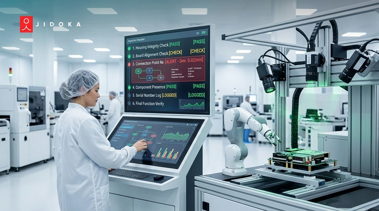
Jidoka transforms this vulnerability using automated optical inspection of PCBs paired with AI. We call this HILDA (Human-In-the-Loop Designed Algorithms). When a machine flags a potential defect, the AI acts as a "Co-Pilot." It presents the image to the operator with a probability score.
Crucially, the system learns from the human's decision. If the operator overrides the AI, the model updates instantly. This creates a self-improving "Golden Loop." The AI gets smarter with every shift. This drastically reduces false alarms in PCB defect detection and ensures circuit board inspection remains accurate over time.
Deploying the Jidoka "AI Suit" Across the SMT Lifecycle
Jidoka Tech solves this by building an AI powered inspection system that performs under real production pressure. Their team aligns cameras, lighting, and PLC timing so the system works across all shifts. This goes beyond standard PCB inspection methods.
Plants running Jidoka’s setup report consistent performance even at extremely high volumes up to 300 million inspections per day. This robustness comes from combining two core systems that extend circuit board inspection capabilities:
1. KOMPASS:高精度検査システム
Kompass は、欠陥検出ロジックの中核を担います。稼働ライン上で99.8%以上の精度を実現し、各フレームを10ミリ秒以内で解析します。
- 適応性: 従来のモデルと比較して、60〜70%少ないサンプル数で新しいバリエーションを学習します。
- 表面検査のスペシャリスト: 反射の強い金属やテクスチャのある部品も容易に処理します。光沢のあるはんだ接合部や銅配線が一般的なカメラでは判別しにくい回路基板の検査に最適です。
- 一貫性: KOMPASSは、視覚的な一貫性が極めて重要な現場での導入をサポートします。
2. NAGARE:工程・組立分析システム
Kompassが部品を検査する一方で、 Nagare は工程を監視します。既存のカメラを活用して組立工程の100%を追跡し、「インテグレーター」として機能します。
- リアルタイムロジック: 部品の欠落や手順の誤りを即座に検知します。
- 根本原因分析: 自動光学検査(AOI)で欠陥が検出された場合、Nagareはその原因を遡って特定します。
- 成果: Nagareを導入した工場では、手直し作業を 20〜35%削減しています。 ステーションのチェック体制と目視検査の自動化を強化することで実現します。
Jidokaは、この包括的なプリント基板検査スイートをローカルのエッジユニット上で実行し、クラウドによる遅延を回避します。これにより、PCBの品質管理を迅速かつ安全に、単一のダッシュボードで一元管理することが可能です。
結論
断片化された基板検査は、水鉄砲で火を消そうとするようなものです。連携の取れていない機械や疲弊した作業員は見落としを招き、旧式の自動光学検査(AOI)システムは誤検知でラインを停止させてしまいます。
たった一つの欠陥流出が利益を食いつぶします。さらに悪いことに、不良品を出荷すればリコールにつながり、顧客の信頼を失墜させます。2025年の今、検査の「死角」は許されません。
Jidoka Technologies は、こうした損失を食い止めます。私たちは、製造ライン全体を接続する統合型「AIスイート」を導入します。印刷工程から最終テストまで検知機能を連携させることで、 Kompass および Nagare が、発生源でエラーを捕捉します。
検査の隙間を埋める準備はできましたか? 今すぐJidokaでプロセスを診断する。
よくある質問
1. プリント基板検査において最も重要なステップは何ですか?
はんだ印刷検査(SPI)は、欠陥の70%がここで発生するため極めて重要です。初期段階でエラーを捕捉することは、基板検査コストの最適化につながります。今すぐ欠陥を検知できれば、低コストで修正可能です。後の工程まで持ち越すと、PCBの欠陥検出コストは跳ね上がります。SPIを優先することで、PCB全体の品質管理が向上し、信頼性の高い基板組み立て検査が実現します。
2. JidokaのAIスイートはどのように誤検知を減らしますか?
JidokaはHILDAを活用して自動光学検査を最適化します。システムは「ゴールデンループ」を通じて作業員のフィードバックから学習します。このプロセスにより、本物のエラーと無害な影を識別し、PCB欠陥検出の精度を向上させます。これにより、良品がAOI検査で誤って弾かれることを防ぎ、チームが真の問題のみに集中できるようになります。
3. Jidokaは既存の機械(Koh YoungやOmronなど)と統合できますか?
はい、Jidokaはハードウェアに依存しないインテグレーターとして機能します。現在お使いのPCB検査手法や装置をそのまま活用いただけます。当社は「AIスーツ」を重ね合わせることで、Koh Youngなどのブランドから得られるデータを統合します。これにより、自動光学検査システムを一つのダッシュボードに集約し、高価なハードウェアを買い替えることなく、回路基板の検査能力をアップグレードできます。
4. なぜ2025年にはX線検査(AXI)が必須となるのか?
その理由は、部品の小型化にあります。BGAのような部品は、標準的なPCB自動光学検査では接合部が隠れて見えません。X線検査は、こうした部品の下を確認できる唯一の手段です。光学的な基板実装検査技術では対応できない構造的な完全性を検証するために不可欠です。高度な回路基板検査において、欠陥ゼロを実現するにはAXIが欠かせません。